Light-transmitting conductor having nanostructure pattern and method for manufacturing same
a technology of light-transmitting conductors and nanostructures, which is applied in the direction of sustainable manufacturing/processing, instruments, and final product manufacturing, etc., can solve the problems of light-transmitting conductors, light transmission and conductivity, and may be incompatible, and it is difficult to have high light transmission and high conductivity at the same tim
- Summary
- Abstract
- Description
- Claims
- Application Information
AI Technical Summary
Benefits of technology
Problems solved by technology
Method used
Image

Examples
embodiment 1
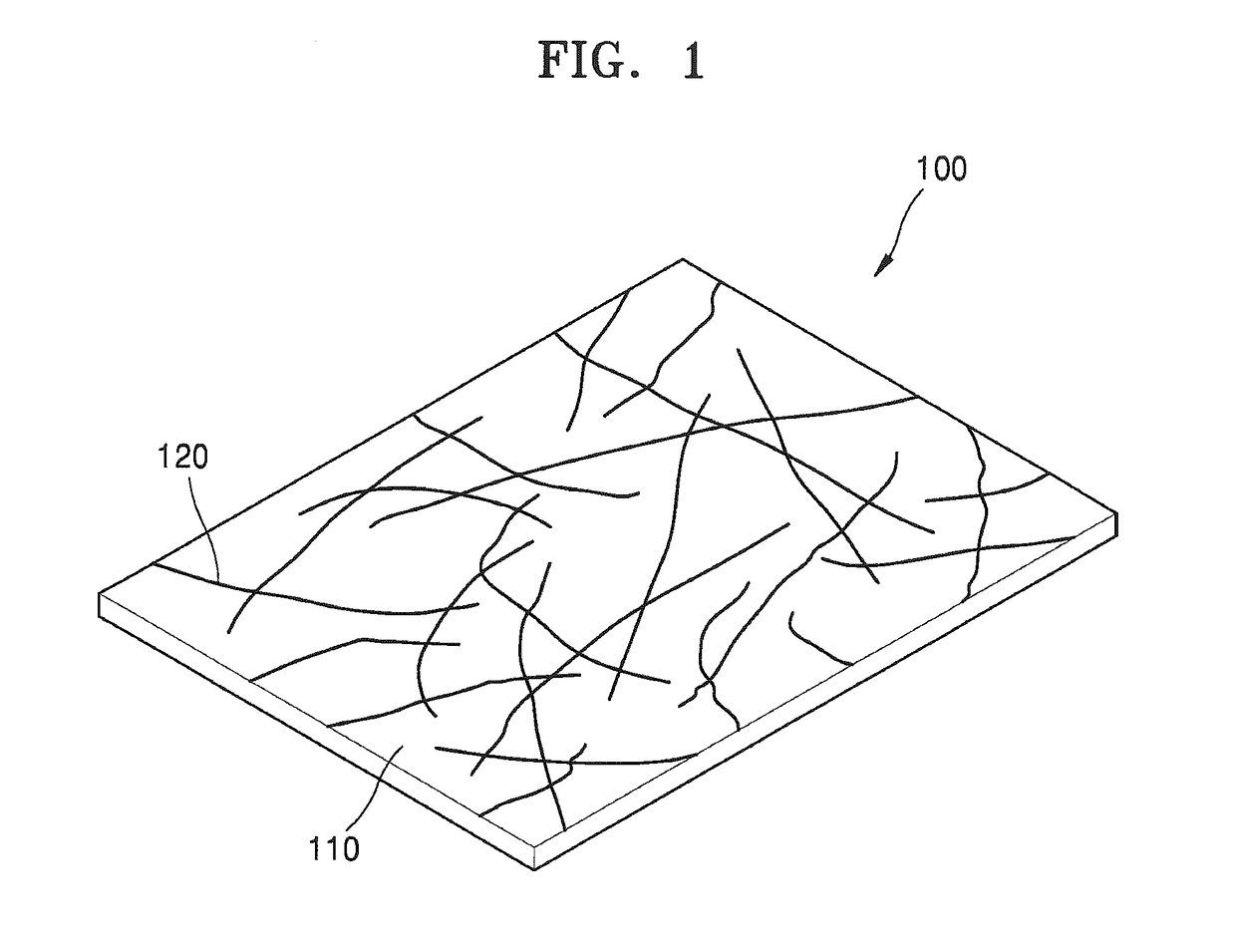
[0052]According to the present embodiment, as shown in FIG. 1, a light-transmitting conductor 100 includes a substrate 110 and a conduction layer 120.
[0053]The light-transmitting conductor 100 may transmit light and be electrically conductive. In this case, it is preferable that light transmittance is at least 90%.
[0054]The conduction layer 120 is formed above the substrate 110 by coating or laminating. The substrate 110 may be rigid or flexible. The substrate 110 may be light-transmitting or non-light-transmitting. The substrate 110 may include a rigid material such as glass, polycarbonate, acryl, etc., or a flexible material such as polyester, polyolefin, polyvinyl, polyimide, silicon, etc. The substrate 110 may include cyclic olefin polymer (COP), cyclic olefin copolymer (COC), or triacetyl cellulose (TAC). However, the substrate 110 is not limited thereto.
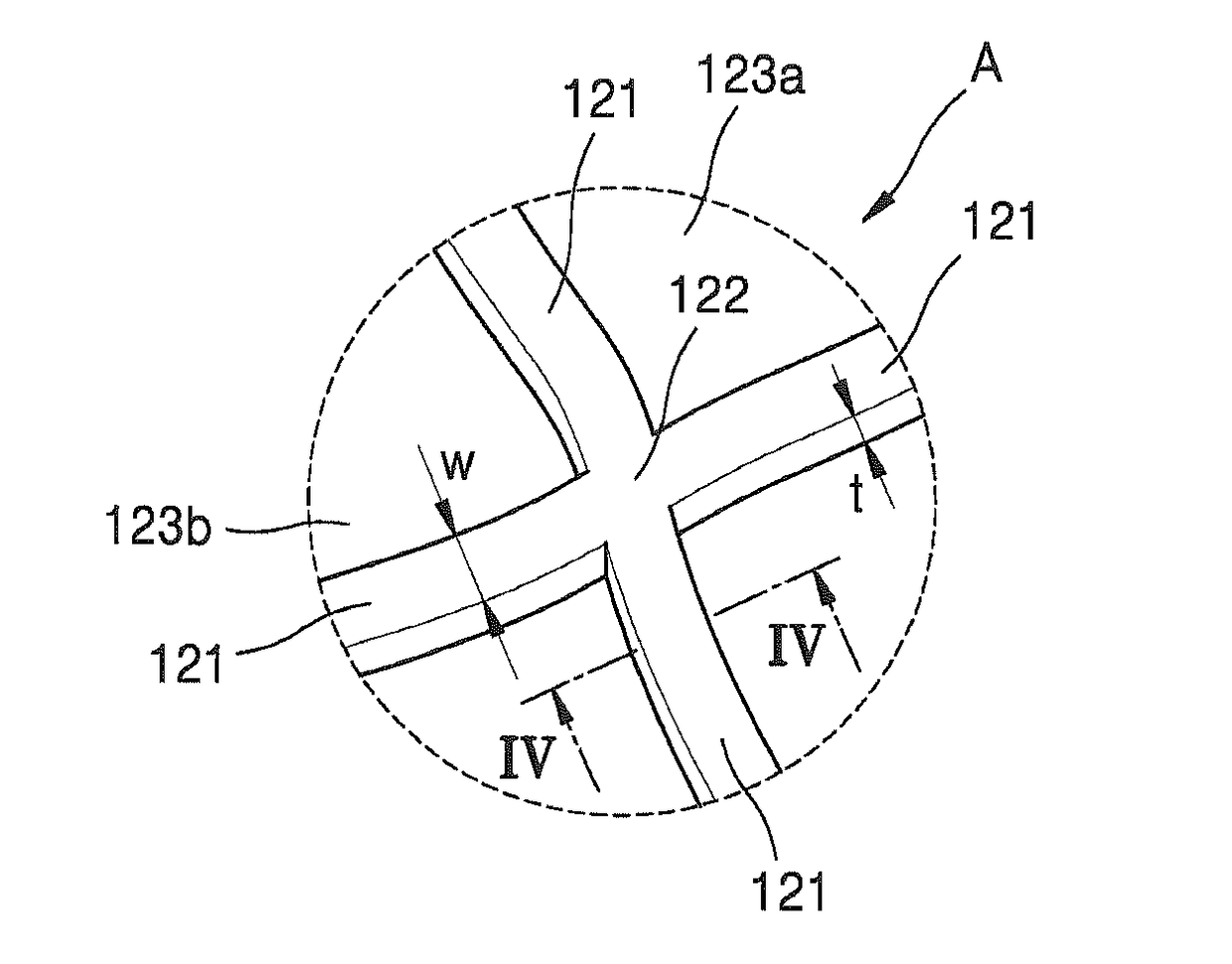
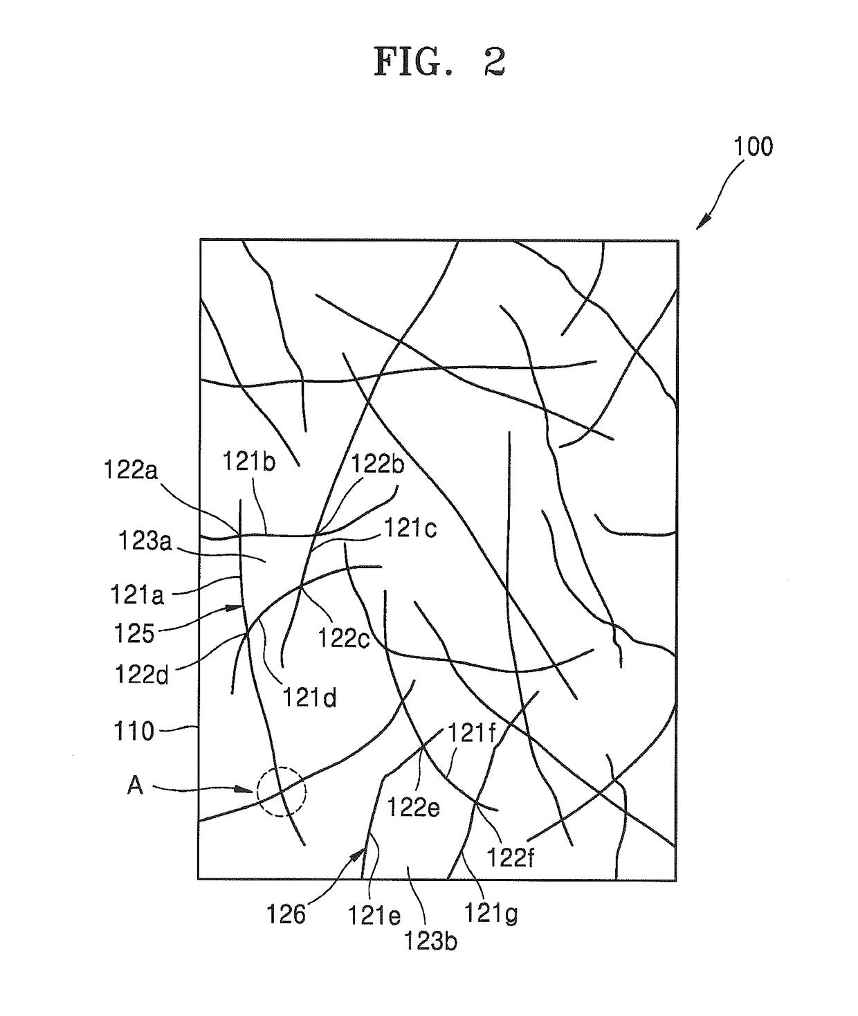
[0055]The conduction layer 120 refers to an electric conduction layer fondled above the substrate 110. The conduction layer 1...
embodiment 2
[0062]According to the present embodiment, as shown in the example of FIG. 5, a conduction layer 220 formed on a substrate 210 of a light-transmitting conductor 200 has a pattern that corresponds to a network formed by intersecting nanostructures. Thus, the conduction layer 220 includes a pattern that includes a main portion 221 and an intersection 222. However, since the main portion 221 consecutively extends from one end of the conduction layer 220 to another end of the conduction layer 220, an end of the main portion 221 does not exist in the pattern.
[0063]Accordingly, electrical connection reliability of the conduction layer 220 may be increased due to the main portion 221 and the intersection 222. Also, since there is no disconnected portions such as an end of the main portion 221, static electricity may be prevented from occurring at disconnected portions.
[0064]According to the present embodiment, the pattern of the conduction layer 220 may be easily formed by using nano-fiber...
embodiment 3
[0065]According to the present embodiment, as shown in the example of FIG. 6, a conduction layer 320 formed on a substrate 310 of a light-transmitting conductor 300 has a pattern that corresponds to a network formed by intersecting nanostructures. Thus, the conduction layer 320 includes a pattern that includes a main portion 321, an intersection 322, and an end 324 of a main portion 321. However, since the main portion 321 does not consecutively extend from one end of the conduction layer 320 to another end of the conduction layer 320, main portions 321a, 321b, and 321c and intersections 322a and 322b may be connected without an evident distinction of inside and outside and thus form an open system 326. However, the main portions 321a, 321b, and 321c and the intersections 322a and 322b cannot form a closed system in which the main portions 321a, 321b, and 321c and the intersections 322a and 322b are connected such that an opening 323 is therein.
[0066]Accordingly, it is possible to f...
PUM
 Abstract
Description
Claims
Application Information
 - R&D Engineer
- R&D Manager
- IP Professional
- Industry Leading Data Capabilities
- Powerful AI technology
- Patent DNA Extraction
Browse by: Latest US Patents, China's latest patents, Technical Efficacy Thesaurus, Application Domain, Technology Topic.
© 2024 PatSnap. All rights reserved.Legal|Privacy policy|Modern Slavery Act Transparency Statement|Sitemap