Display driver and method for driving display device

Active Publication Date: 2017-06-01
LAPIS SEMICON CO LTD
View PDF0 Cites 0 Cited by
  • Summary
  • Abstract
  • Description
  • Claims
  • Application Information

AI Technical Summary

Benefits of technology

[0013]Thus, according to the present invention, a period spent for the correction processing and the display driving processing can be prolonged as compared to a case where the correction processing for correcting the characteristic of the drive transistor is perf

Problems solved by technology

Due to element delay, the above-described correction offset voltages can no longer reach desired voltage values and it becomes difficult to have a sufficient emission period for causing the

Method used


Image

  • Display driver and method for driving display device
  • Display driver and method for driving display device
  • Display driver and method for driving display device

Examples


Example

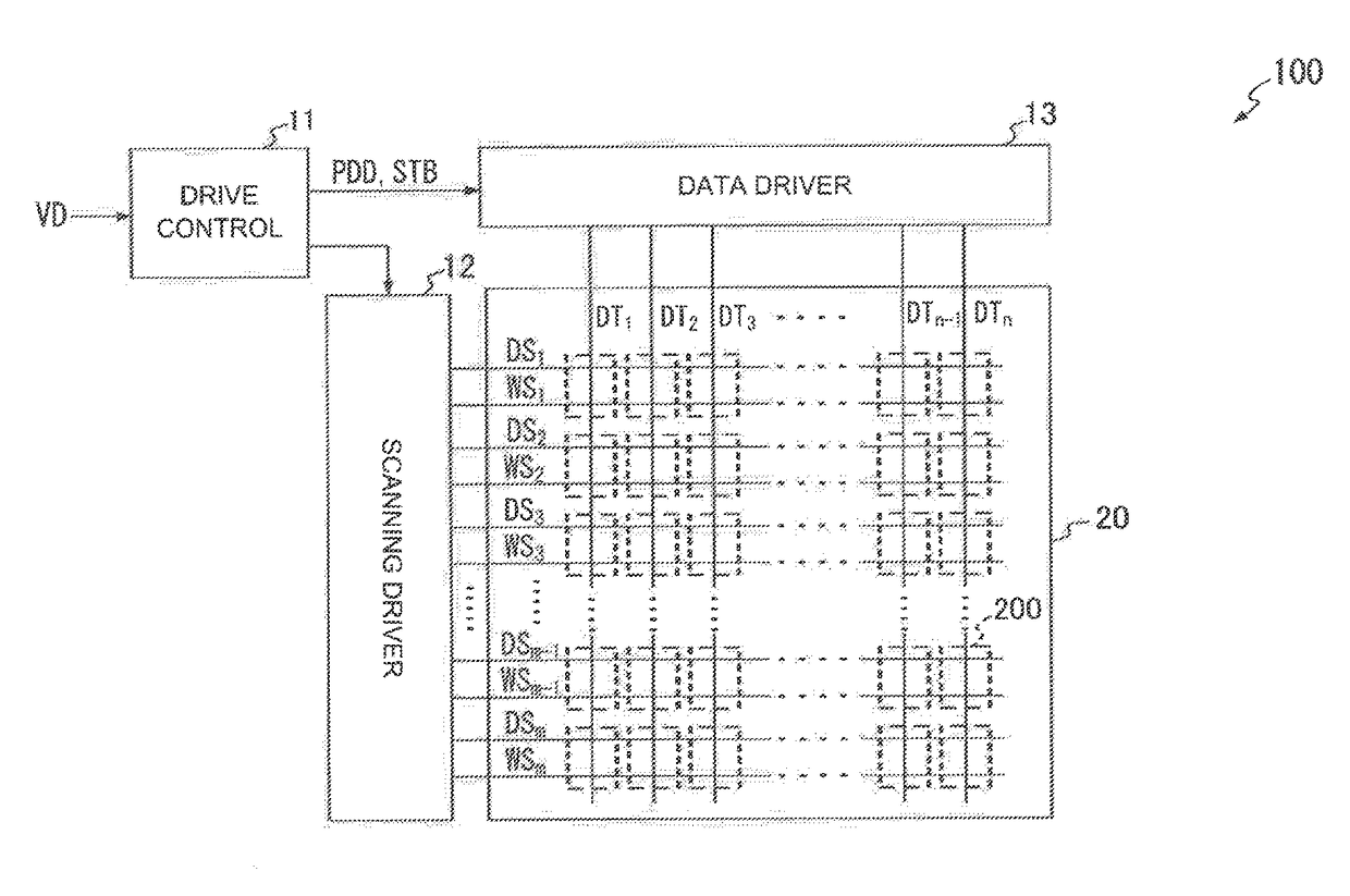
[0021]FIG. 1 is a block diagram illustrating a general configuration of an EL display apparatus 100 including a display driver according to the present invention. In FIG. 1, a display device 20 includes an organic EL panel, for example. The display device 20 includes m (m is a natural number greater than or equal to 2) write control lines WS1 to WSm and m power-supply lines DS1 to DSm extending in a horizontal direction of a two-dimensional screen and n (n is an even number greater than or equal to 2) data lines DT1 to DTn extending in a vertical direction of the two-dimensional screen. At intersections (i.e., regions surrounded by broken lines) between the write control lines WS and the data lines DT, display cells 200, which function as pixels, are formed. Note that a pair of a write control line WS(k) (k is an integer of 1 to n) and a power-supply line DS(k) forms one horizontal scanning line.

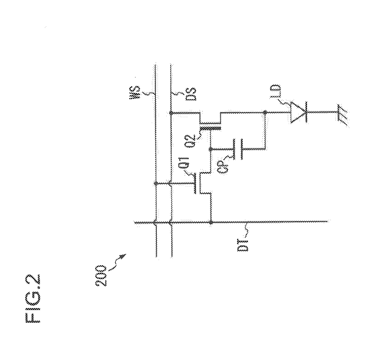
[0022]FIG. 2 is a circuit diagram illustrating an example of the internal configuration ...


PUM


Abstract

Only once every N horizontal scanning periods, correction processing for providing a correction voltage for correcting a characteristic of a drive transistor for driving a light-emitting element formed in a display device to data lines of the display device and display driving processing for sequentially providing, to the data lines of the display device, gradation voltages for one horizontal scanning line based, on a video signal corresponding to each of N horizontal scanning lines are executed.

Description

BACKGROUND OF THE INVENTION[0001]1. Field of the Invention[0002]The present invention relates to a display driver for driving a display device and a method for driving a display device.[0003]2. Description of the Related Art[0004]Currently known flat (or flat panel) display devices include an organic electroluminescence (EL) panel employing organic EL elements as pixels.[0005]Each pixel in an active matrix-driven organic EL panel includes an organic EL element and a drive transistor for providing, to the organic EL element, a driving current to cause the organic EL element to emit light. The drive transistor is typically a thin film transistor using polysilicon or amorphous silicon, for example. Such thin film transistors, however, have large variations in carrier mobility and threshold voltage.[0006]In view of this, there has been proposed a driving method for driving an organic EL panel according to which drive transistors are driven as follows for each horizontal scanning period ...

Claims


Application Information

Patent Timeline
IPC IPC(8): G09G3/3241G09G3/3291G09G3/3266
CPCG09G3/3241G09G3/3266G09G2300/0408G09G2310/08G09G2300/0819G09G3/3291G09G3/3225G09G3/3233G09G2300/0842G09G2310/0294G09G2310/0297G09G2320/043
Inventor NITAWAKI, SHOUJI
Owner LAPIS SEMICON CO LTD
Why Eureka
Try Eureka