Charged Particle Beam Device and Method for Adjusting Position of Detector of Charged Particle Beam Device

Active Publication Date: 2021-09-23
HITACHI HIGH-TECH CORP
View PDF0 Cites 1 Cited by
  • Summary
  • Abstract
  • Description
  • Claims
  • Application Information

AI Technical Summary

Benefits of technology

[0013]In a charged particle beam device including a deceleration optical system, a change in a deceleration electric field and an axis shift d

Problems solved by technology

However, chromatic aberration generally increases in a low acce

Method used


Image

  • Charged Particle Beam Device and Method for Adjusting Position of Detector of Charged Particle Beam Device
  • Charged Particle Beam Device and Method for Adjusting Position of Detector of Charged Particle Beam Device
  • Charged Particle Beam Device and Method for Adjusting Position of Detector of Charged Particle Beam Device

Examples


Example

[0025]Hereinafter, an embodiment of the invention will be described with reference to the accompanying drawings. Although the accompanying drawings show a specific embodiment in accordance with principles of the invention, the present embodiment is provided for a purpose of understanding the invention, and is not used for limiting interpretation of the invention. In all the drawings showing the present embodiment and modifications, those having the same function are designated by the same reference numerals, and the repeated description thereof will be omitted.

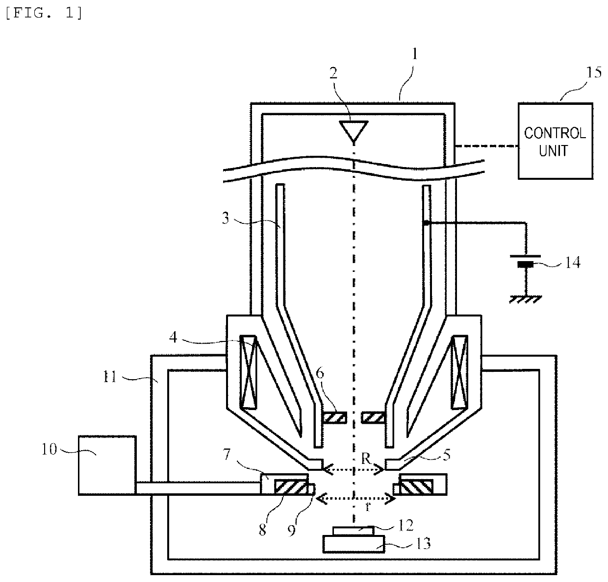
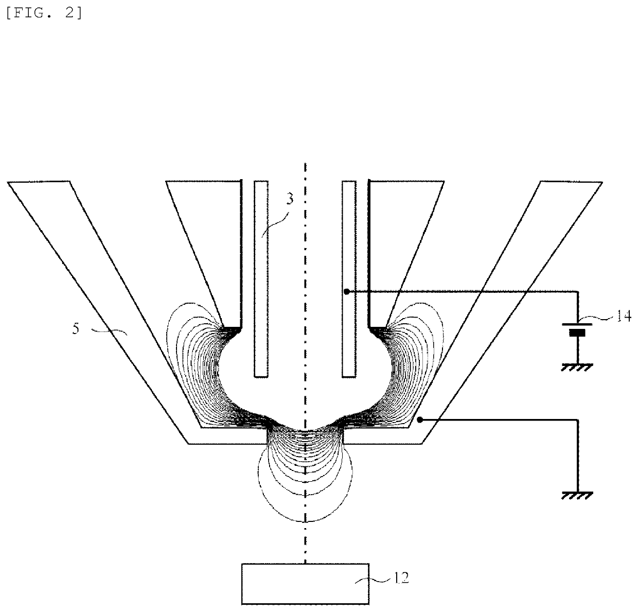
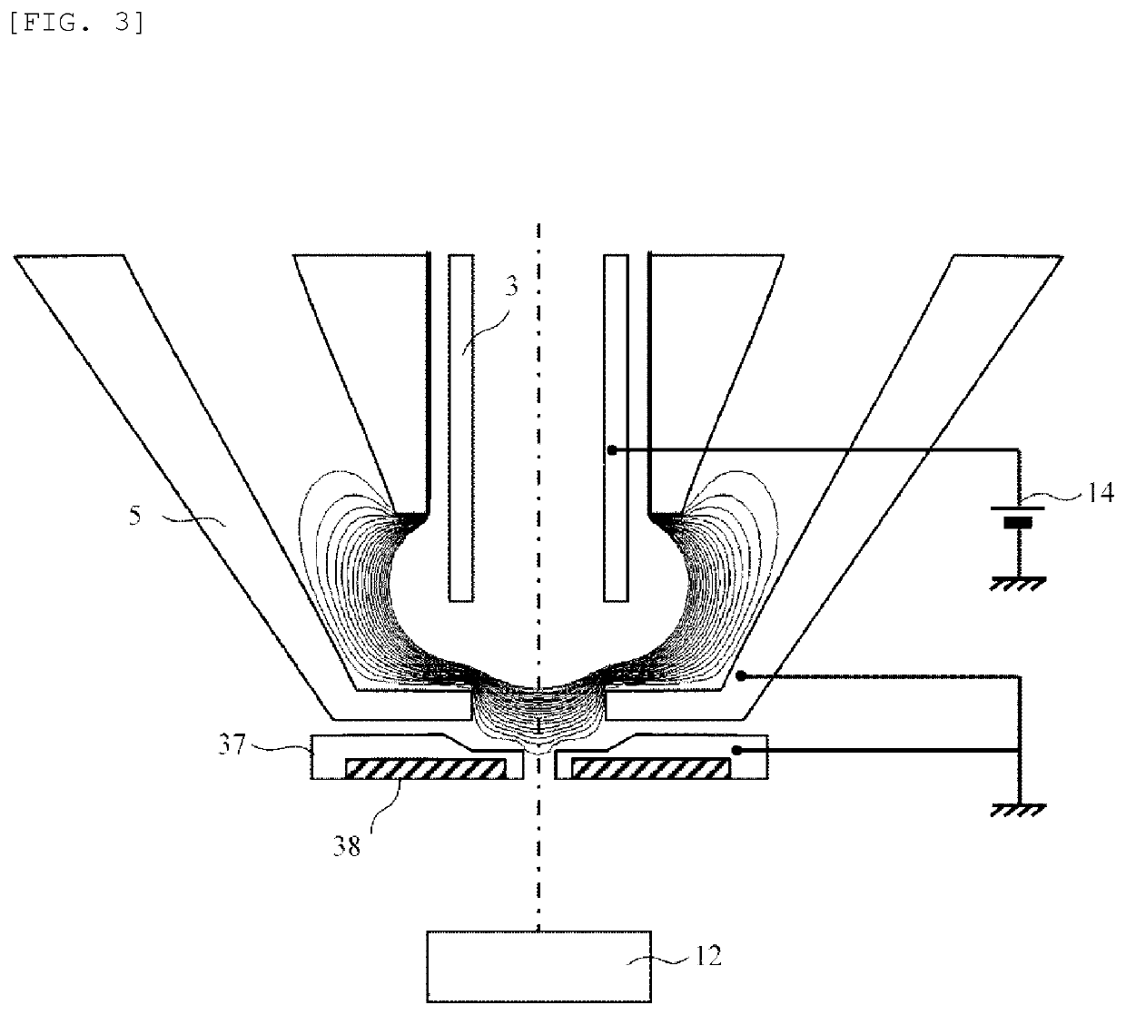
[0026]FIG. 1 is a schematic cross-sectional view showing a charged particle beam device according to the present embodiment. An SEM to which a boosting method is applied is shown as an example of the charged particle beam device. An SEM column 1 includes an electron source 2 including a mechanism that irradiates a sample 12 with a probe electron beam, an electronic lens such as a condenser lens (not shown) and an objective len...


PUM


Abstract

In a charged particle beam device including a deceleration optical system, a change in a deceleration electric field and an axis shift due to a structure between an objective lens and a sample are prevented to reduce adverse effects on an irradiation system and detection system. The charged particle beam device includes an electron source, an objective lens configured to focus a probe electron beam from the electron source on the sample, an acceleration electrode configured to accelerate the probe electron beam, a first detector provided in the acceleration electrode, a deceleration electrode configured to form a deceleration electric field for the probe electron beam with the acceleration electrode, the probe electron beam being configured to pass through an opening of the deceleration electrode, and a second detector inserted between the deceleration electrode and the sample. The second detector includes an opening portion larger than the opening of the deceleration electrode, and a sensing surface is provided around the opening portion.

Description

TECHNICAL FIELD[0001]The present invention relates to a charged particle beam device and a method for adjusting a position of a detector of the charged particle beam device.BACKGROUND ART[0002]A scanning electron microscope (SEM) obtains a two-dimensional image of a region to be scanned on a sample surface by detecting signal electrons generated when a sample is irradiated and scanned with a focused probe electron beam and displaying a signal intensity of each irradiation position in synchronization with a scanning signal of the irradiation electron beam.[0003]In recent years, low acceleration observation with irradiation energy of about 1 keV or less is increasingly important for a purpose of avoiding charging or damage of the sample due to the electron beam irradiation during SEM observation and obtaining sample information on an electrode surface. However, chromatic aberration generally increases in a low acceleration region, and it is difficult to obtain high resolution. In orde...

Claims


Application Information

Patent Timeline
IPC IPC(8): H01J37/145H01J37/244H01J37/20H01J37/28H01J37/26
CPCH01J37/145H01J37/244H01J2237/04756H01J37/28H01J37/265H01J37/20H01J2237/1502H01J2237/24475
Inventor IMAI, YUTASASAJIMA, MASAHIROTAKAHOKO, YOSHIHIRO
Owner HITACHI HIGH-TECH CORP
Why Eureka
Try Eureka