Low temperature poly-silicon TFT substrate

a thin film transistor and low temperature technology, applied in the field of display technology, can solve the problems of lowering manufacturing efficiency, leakage current, abnormal panel display, etc., and achieve the effects of reducing one photo-mask, preserving the stability of the tft device, and saving the manufacturing process of the shielding metal layer

Active Publication Date: 2017-06-08
SHENZHEN CHINA STAR OPTOELECTRONICS TECH CO LTD +1
View PDF5 Cites 12 Cited by
  • Summary
  • Abstract
  • Description
  • Claims
  • Application Information

AI Technical Summary

Benefits of technology

[0028]The efficacy of the present invention is that the present invention provides a LTPS TFT substrate, which comprises a black matrix arranged on a first buffer layer of the LTPS TFT substrate to have an area where a TFT device is located is shielded by the black matrix thereby preventing the TFT device from being influenced by light irradiation, maintaining stability of the TFT device; and also savi

Problems solved by technology

However, when influenced by light irradiation, poly-silicon may cause instability of device, leading to an increase of leakage current and causi

Method used


Image

  • Low temperature poly-silicon TFT substrate
  • Low temperature poly-silicon TFT substrate
  • Low temperature poly-silicon TFT substrate

Examples


Embodiment Construction

[0033]To further expound the technical solution adopted in the present invention and the advantages thereof, a detailed description is given to a preferred embodiment of the present invention and the attached drawings.

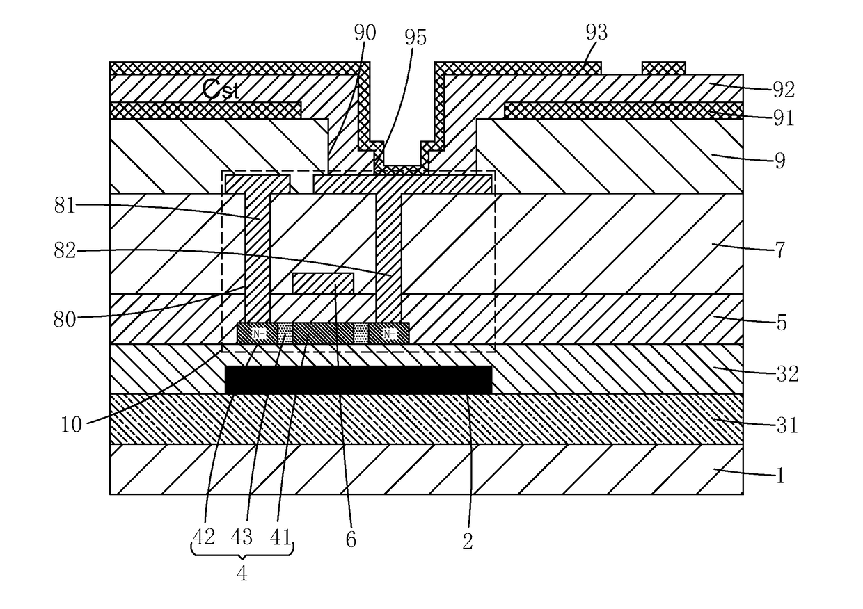
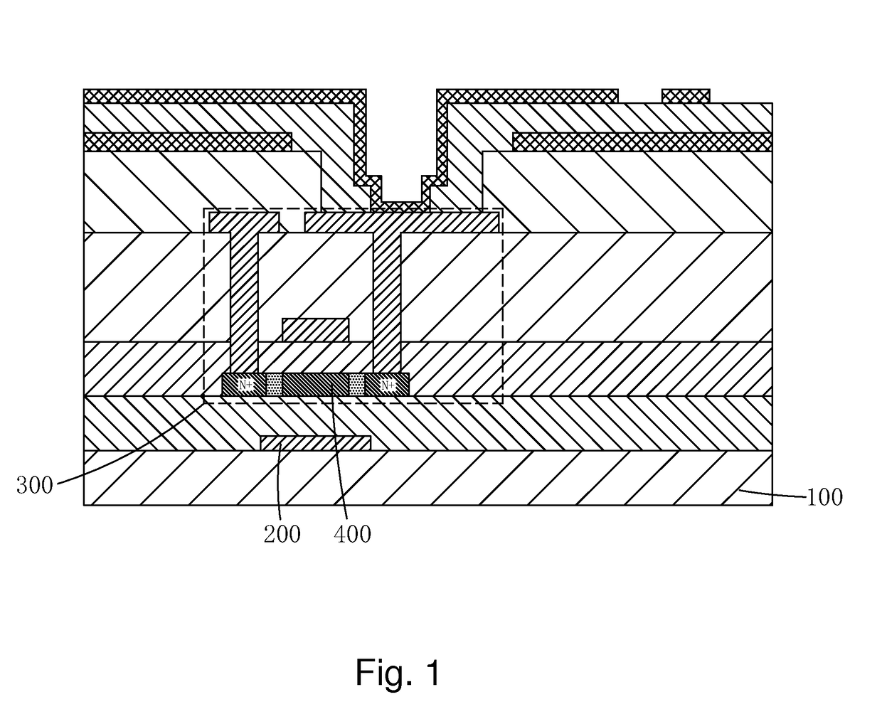
[0034]Referring to FIG. 2, the present invention provides a low temperature poly-silicon (LTPS) thin-film transistor (TFT) substrate, which comprises a base plate 1, a first buffer layer 31 formed on the base plate 1, a black matrix 2 formed on the first buffer layer 31, a second buffer layer 32 formed on the first buffer layer 31 and the black matrix 2, a poly-silicon layer 4 formed on the second buffer layer 32, a gate insulation layer 5 formed on the poly-silicon layer 4, a gate electrode 6 formed on the gate insulation layer 5, an interlayer insulation layer 7 formed on the gate insulation layer 5 and the gate electrode 6, a source electrode 81 and a drain electrode 82 formed on the interlayer insulation layer 7, a planarization layer 9 formed on the interlayer ins...


PUM


Abstract

The present invention provides a LTPS TFT substrate, which includes a black matrix arranged on a first buffer layer of the LTPS TFT substrate to have an area where a TFT device is located is shielded by the black matrix thereby preventing the TFT device from being influenced by light irradiation, maintaining stability of the TFT device; and also saving the manufacturing process of a shielding metal layer, reducing one photo-mask, and lowering down manufacturing cost so as to allow the black matrix, in achieving the functionality of its own (shielding leaking light of the pixel), to also take the place of a shielding metal layer that is commonly adopted in the prior art to shield light for the TFT device and thus providing duality of functionality.

Description

BACKGROUND OF THE INVENTION[0001]1. Field of the Invention[0002]The present invention relates to the field of display technology, and in particular to a low temperature poly-silicon thin-film transistor (TFT) substrate.[0003]2. The Related Arts[0004]Low temperature poly-silicon (LTPS) thin-film transistors (TFTs) have a great value of application and potential in the fields of active matrix liquid crystal display (AMLCD) and active-matrix organic light emitting diode (AMOLED) display that have a high resolution.[0005]Compared to the amorphous silicon (a-Si) technology, LTPS TFT has a high mobility and excellent device stability. The mobility of LTPS TFT may get as high as tens to hundreds cm2 / Vs, well suiting the needs for AMLCD and AMOLED having a high resolution. Thus, the LTPS display devices have a high response speed and various advantages of for example high brightness, high resolution, and low power consumption. Besides serving as a pixel switch, an LTPS TFT may also be used ...

Claims


Application Information

Patent Timeline
IPC IPC(8): G02F1/1362H01L29/786G02F1/1368
CPCG02F1/136209G02F1/136213G02F1/1368G02F2001/136231H01L29/78621G02F2001/13685G02F2202/104G02F1/136227H01L27/1214H01L29/78633H01L29/78675H01L27/124H01L27/1255G02F1/136231G02F1/13685
Inventor XU, YONG
Owner SHENZHEN CHINA STAR OPTOELECTRONICS TECH CO LTD
Why Eureka
Try Eureka