Eureka AIR delivers breakthrough ideas for toughest innovation challenges, trusted by R&D personnel around the world.

Marking method for wafer dice

a technology of wafer dies and marking methods, which is applied in the direction of manufacturing tools, welding/soldering/cutting articles, and semiconductor/solid-state device details, etc., can solve the problems of difficult to mark the wafer dies on the accurate position of each of the divided wafer dies, and the damage of the wafer, etc., to achieve the effect of quick collection

Active Publication Date: 2017-06-08
TECHNICS
View PDF0 Cites 1 Cited by
  • Summary
  • Abstract
  • Description
  • Claims
  • Application Information

AI Technical Summary

Benefits of technology

The present invention allows for quick and accurate collection of information about the shape and position of wafer dies that are divided in a dicing process and arranged irregularly. This information is used to perform accurate marking on each individual die.

Problems solved by technology

However in this method, in the wafer dicing process fragments or chippings may be generated from the back surface of the wafer or the wafer may be damaged.
However, as the divided wafer dies are located askew from the original positions on the wafer, it is difficult to mark the wafer dies on an accurate position of each of the divided wafer dies with the conventional marking method using the two wafer dies, namely, the first and second reference wafer dies, for marking the rest wafer dies.
Accordingly, it takes a long time.

Method used


Image

  • Marking method for wafer dice
  • Marking method for wafer dice
  • Marking method for wafer dice

Examples


Embodiment Construction

Technical Problem

[0005]Provided is a method in which the position information of wafer dies which are divided in a dicing process is accurately measured and laser marking is performed by using a line scan camera.

Advantageous Effects of the Invention

[0006]According to embodiments of the present invention, the shape and position information of wafer dies which are divided in a dicing process and arranged irregularly can be quickly collected by using a line scan camera. If a laser marking job is performed based on the thus-collected shape and position information of the wafer dies, marking can be accurately performed on a required location of each of the divided wafer dies.

DESCRIPTION OF THE DRAWINGS

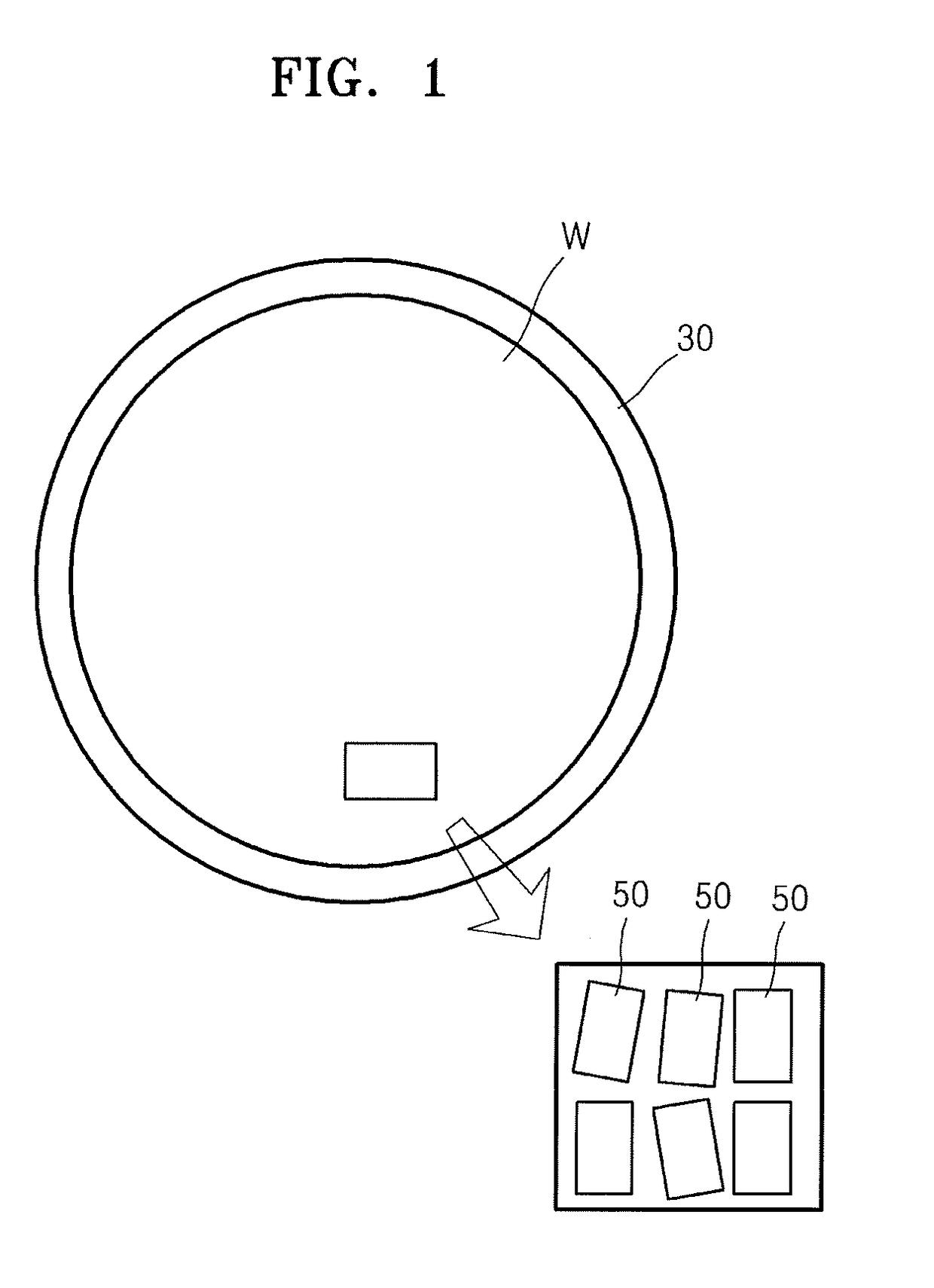
[0007]FIG. 1 shows wafer dies arranged irregularly after a wafer is divided in a dicing process.

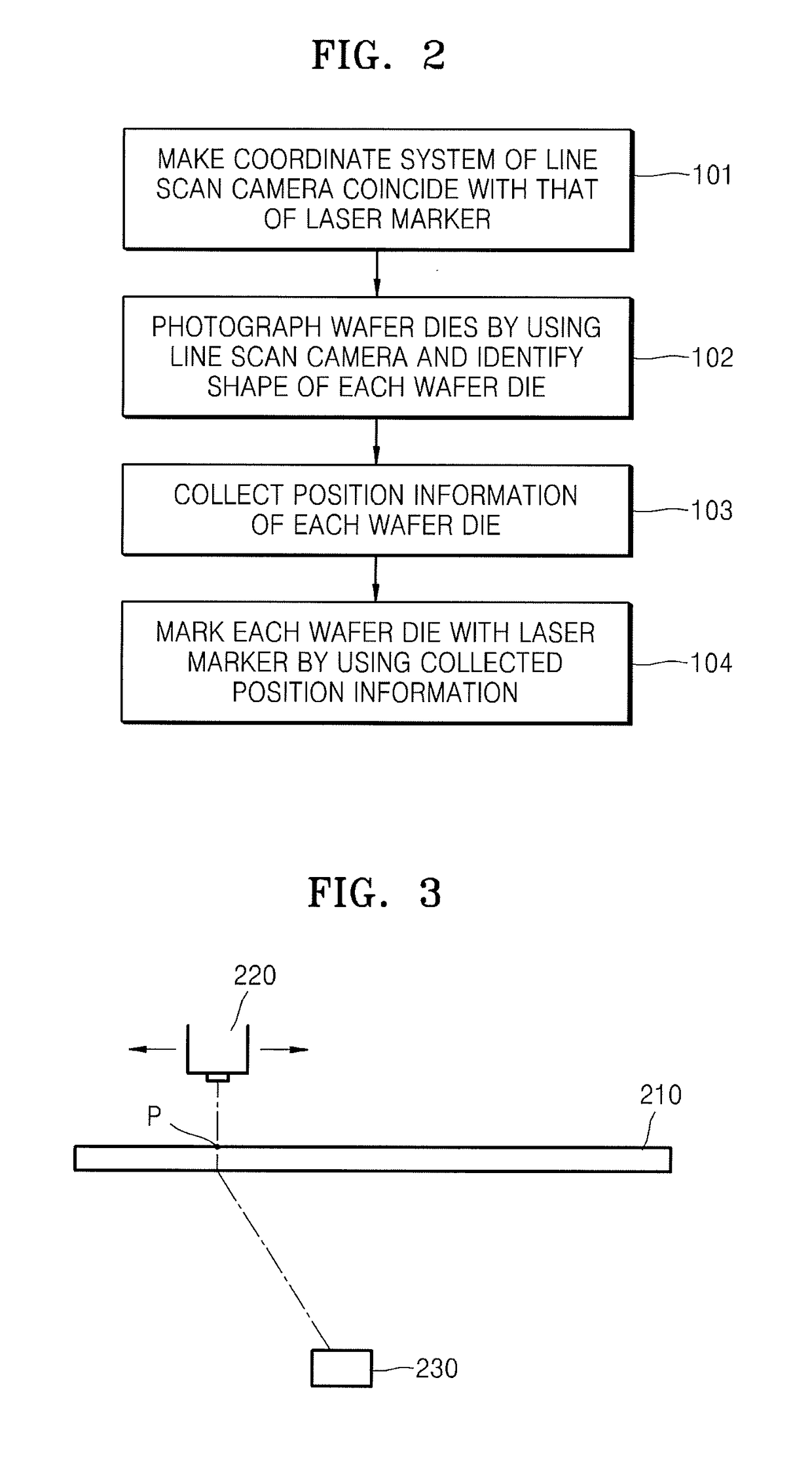
[0008]FIG. 2 is a flowchart of a marking method of wafer dies according to an embodiment of the present invention.

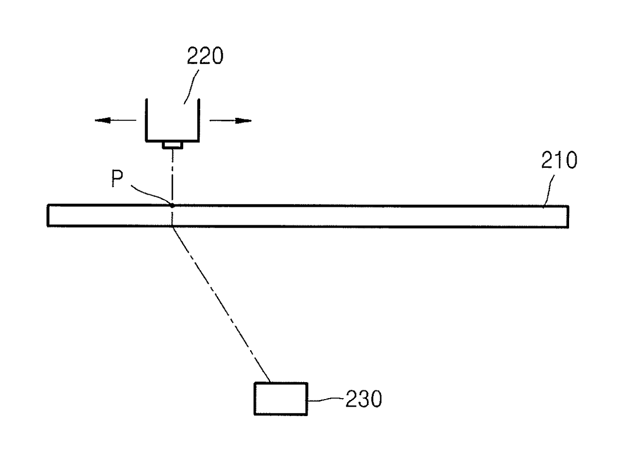
[0009]FIG. 3 illustrates a method of making the coordinate system of a line scan ...


PUM

PropertyMeasurementUnit
diameteraaaaaaaaaa
diameteraaaaaaaaaa
shapeaaaaaaaaaa

Abstract

Disclosed is a method for marking, by using a laser marker, a plurality of wafer dice divided by a wafer dicing process. The disclosed marking method for wafer dice comprises the steps of: setting a plurality of scan regions having a mutually overlapping portion on a wafer including the wafer dice; scanning the scan regions of the wafer a plurality of times by using a line scan camera; collecting position information of each of wafer dice located in regions in which the scan regions do not overlap; collecting, through image synthesis, position information of each of wafer dice located in regions in which the scan regions overlap; and marking, by using the laser marker, each of all the wafer dice of which the position information has been collected.

Description

TECHNICAL FIELD[0001]The present invention relates to a marking method of wafer dies, and more particularly, to a method of marking wafer dies with a laser in which wafer dies which are divided after a wafer dicing process are marked with a laser after the position information is confirmed by using a line scan camera.BACKGROUND ART[0002]According to conventional technologies, the following method has been used as a laser marking method of wafer dies. First, the back surface of a wafer in which wafer dies are integrated is made to have a desired thickness through backgrinding, and then, two wafer dies are selected as first and second reference wafer dies among wafer dies on the front surface of the wafer. By using the thus-selected first and second reference wafer dies, positions of all the rest wafer dies are identified and then, by using thus-identified position information, each wafer die is marked with a laser. Then, by dicing the wafer, the marked wafer dies are divided. However...

Claims


Application Information

Patent Timeline
Patent Type & Authority Applications(United States)
IPC IPC(8): H01L21/67B23K26/03H01L21/268B23K26/00H01L21/78H01L23/544
CPCH01L21/67282H01L21/78H01L23/544B23K2201/40B23K26/0087B23K26/032H01L2223/5446H01L21/268B23K26/0006B23K26/0869B23K26/359B23K2101/40B23K2103/56H01L2223/54433H01L2924/0002H01L2924/00
Inventor KIM, SUN JUNGCHOI, JAE MANJUNG, SUNG BEOMSEO, JUNG JIN
Owner TECHNICS
Why Eureka
Eureka Blog
Learn More