Electron microscope device and imaging method using same

a technology of electron microscope and imaging method, which is applied in the direction of basic electric elements, electric discharge tubes, electrical equipment, etc., can solve the problems of blurred combined images, high labor and time, and distortion of images,

Active Publication Date: 2017-06-15
HITACHI HIGH-TECH CORP
View PDF10 Cites 7 Cited by
  • Summary
  • Abstract
  • Description
  • Claims
  • Application Information

AI Technical Summary

Benefits of technology

[0014]According to one aspect of the present invention, it is possible to provide an electron microscope device capable of acquiring a high-image-quality wide field image for a relatively short time with respect to imaging of an electron microscope, and an imaging method using it. Moreover, it is possible to provide an electron microscope device capable of automatically setting a dose amount per pixel in the narrow field region or the wide field region properly, and an imaging method using it.

Problems solved by technology

Although in the case of the high-speed scanning, there is little influence of the drift of a stage or a beam, in the case of the low-speed scanning, distortion of an image occurs because the imaging position of the structure in the image shifts during the scanning.
Meanwhile, although a high-speed scanning mode has small distortion, since dislocation between frames cannot be eliminated, if the images are integrated as they are, there will be a problem that a combined image will be blurred.
For this reason, conventionally, an imaging method of re-imaging a region that is wished to be observed in detail at a high magnification after acquiring the whole image at a low magnification is taken; it poses problems that the imaging requires much labor and time.

Method used


Image

  • Electron microscope device and imaging method using same
  • Electron microscope device and imaging method using same
  • Electron microscope device and imaging method using same

Examples


example 1

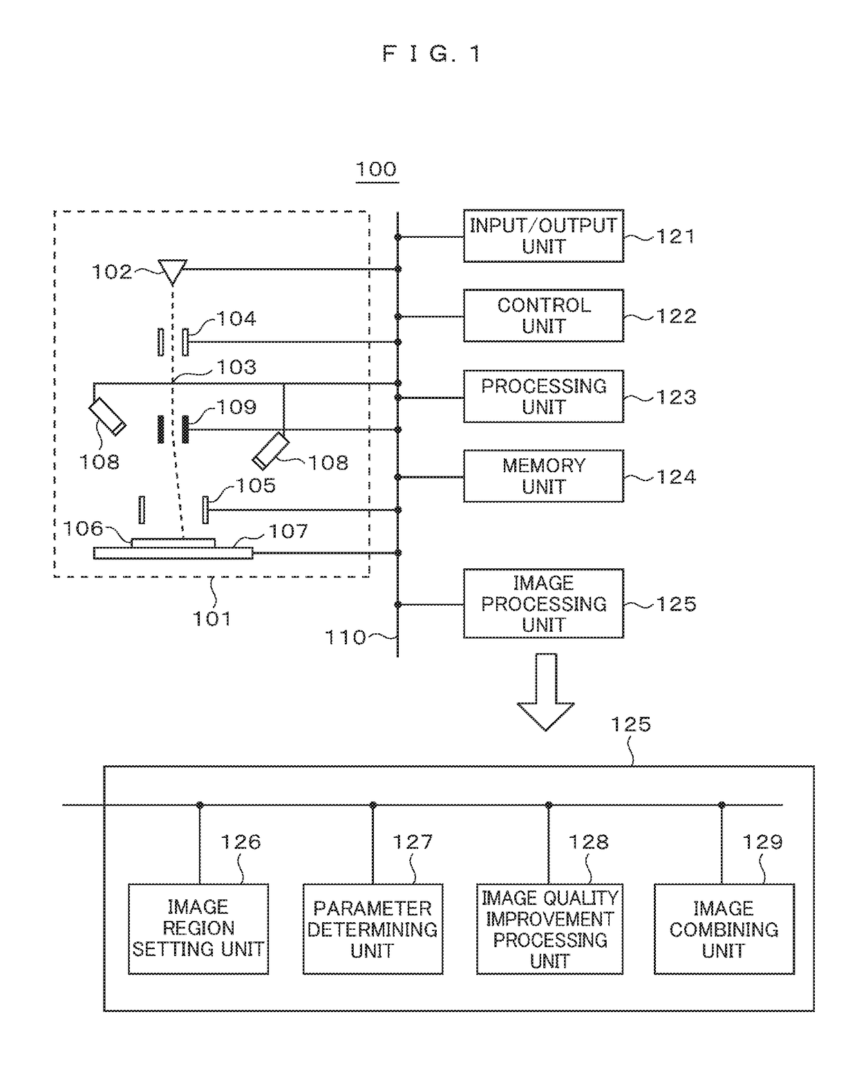
[0047]A first example of the present invention is described using FIGS. 1 to 8. FIG. 1 shows a basic configuration of a scanning electron microscope device 100 that is one embodiment of the present invention. The scanning electron microscope device 100 is configured with, for example, a scanning electron microscope 101, an input / output unit 121, a control unit 122, a processing unit 123, a memory unit 124, and an image processing unit 125.

[0048]The electron image acquisition device 101 generates an electron beam 103 from an electron gun 102, and focuses it on a surface of a sample 106 by making this electron beam 103 pass through a condenser lens 104 and an objective lens 105. Next, it acquires an image by detecting particles generated from the sample 106 on which the electron beam 103 was irradiated with a detector 108. The image is stored in the memory unit 124.

[0049]Multiple of the detectors 108 may be provided, and further the following alternatives may be allowed: the multiple ...

example 2

[0102]A point in which a second example differs from the first example is that in each frame image, each of the narrow field region and the wide field region other than it are imaged with the dose amount adjusted to acquire a frame-integrated image. Moreover, a point in which the second example differs from the first example lies in a point that the narrow field region is set and updated to be larger than the structure by a maximum drift amount that may occur in a next frame image and the next frame image is acquired. Since the scanning electron microscope device used in the second example is the same as the scanning electron microscope device 100 explained using FIG. 1 in the first example, an explanation of a device configuration is omitted. A point in which the second example differs from the first example is explained using FIG. 9 and FIG. 10.

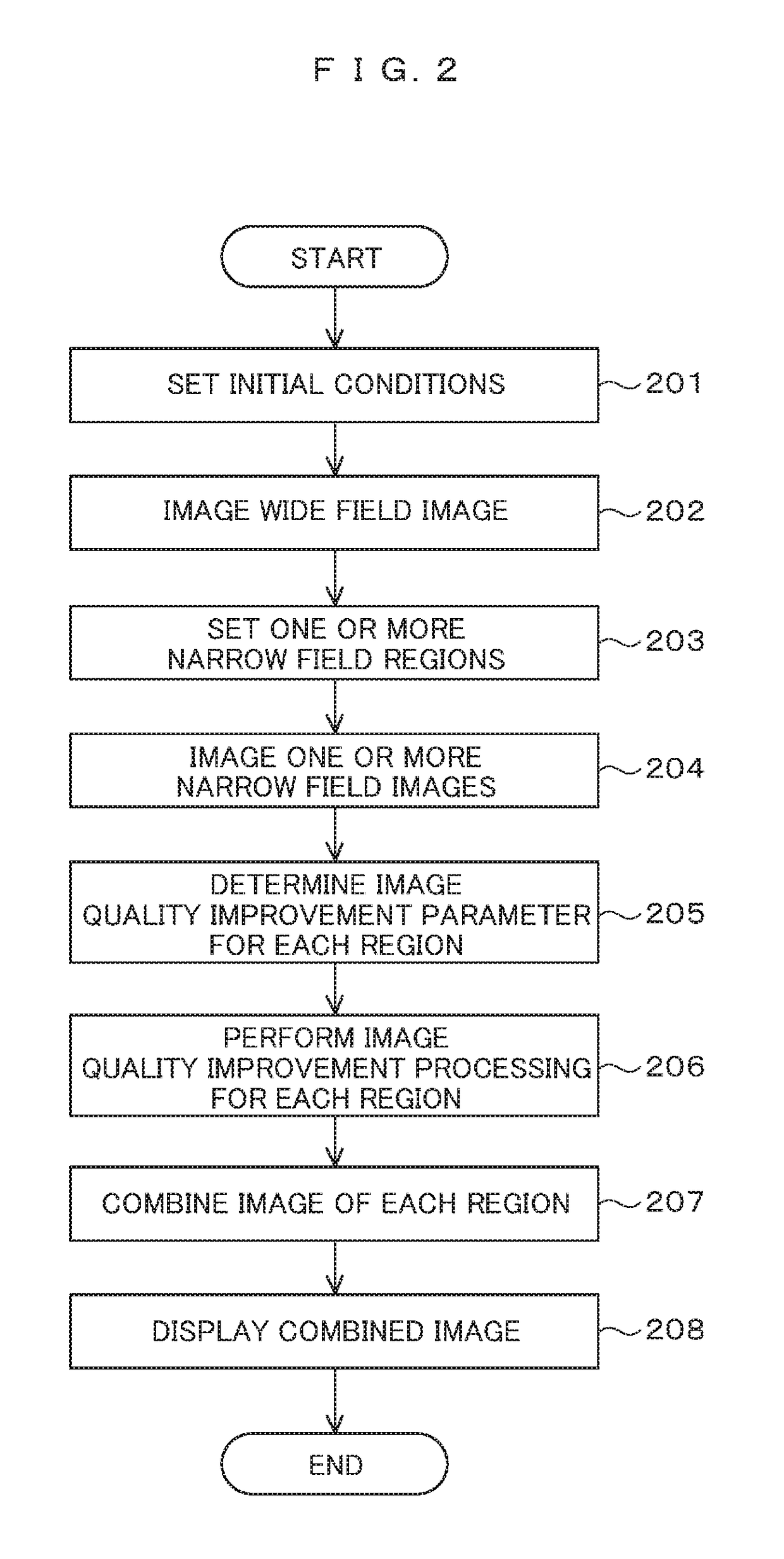
[0103]FIG. 9 is a diagram showing a flow of processing of the second example, and is a diagram of one example showing an example in which ...


PUM


Abstract

In order to enable high-speed imaging of a wide-field image, the imaging method using the electron microscope comprises: irradiating and scanning a wide-field region of the sample with a low-dose amount of electron beam, and acquiring a wide-field image of the sample; setting, from this wide-field image, a narrow-field region; irradiating and scanning this narrow-field region with a high-dose amount of the electron beam, and acquiring a narrow-field image of the sample; determining the noise-removal parameters for the acquired wide-field image and narrow-field image; performing image quality improvement processing on the wide-field image and the narrow-field image; performing drift correction on the narrow-field image undergone the image quality improvement processing; and combining the narrow-field image undergone this drift correction and the wide-field image in such a manner that the visibility of each is at the same level throughout the entirety of the combined image.

Description

TECHNICAL FIELD[0001]The present invention relates to an electron microscope device for imaging a wide field region with a high image quality at a high speed with an electron microscope, and an imaging method using it.BACKGROUND ART[0002]The electron microscope has an extremely high resolution compared with optical microscopes, and is widely used in order to observe a detailed structure of an object to be observed clearly. The electron microscope acquires an image of an object sample by irradiating an electron beam onto the object sample and detecting particles (electrons of the same kind or of a different kind of the irradiated electrons, or electric magnetic wave, or photons) emitted from the object sample or penetrating the object sample with a detector. Observation objects of the electron microscope include materials, semiconductors, food, biotechnology, medical fields, etc.[0003]In inspections and analyses using the electron microscope, there is a demand of wishing to check a w...

Claims


Application Information

Patent Timeline
Patent Type & Authority Applications(United States)
IPC IPC(8): H01J37/26H01J37/244
CPCH01J37/265H01J37/244H01J37/263H01J37/28H01J2237/221H01J2237/24592H01J2237/2809H01J2237/2817
Inventor KOBAYASHI, MITSUTOSHINAKAHIRA, KENJITANAKA, MAKI
Owner HITACHI HIGH-TECH CORP
Why Eureka
Try Eureka