
Touch display panel and display device

Active Publication Date: 2017-06-22
SHANGHAI TIANMA MICRO ELECTRONICS CO LTD +1
View PDF6 Cites 15 Cited by
  • Summary
  • Abstract
  • Description
  • Claims
  • Application Information

AI Technical Summary

Benefits of technology

The patent text describes a technology that improves the display of touch display panels by increasing the amount of light that can pass through the panel, reducing the impact of color distortion. This results in a more effective and transparent display.

Problems solved by technology

However, technology is complex and cost is high when manufacturing a component for integrating a touch panel with a liquid crystal panel under high resolution of pixel.
It is a major problem perplexing industries for manufacturing in-cell touch liquid crystal panels under high resolution of pixel by utilizing a low-cost technology.
The existing structures 1 and 2 would lower transmittance of a display panel, and the existing structures 4 and 3 would partially enhance transmittance of a display panel, but is likely to cause serious color offset of a display panel.
In addition, liquid crystals at a connecting part where the touch electrode and the touch line are connected via a through hole cannot be effectively controlled by an electric field, i.e., black domain lines are likely to occur at c1 in FIG. 1, resulting in decrease of aperture ratio of a display panel and influence on display effect.

Method used


Image

  • Touch display panel and display device
  • Touch display panel and display device
  • Touch display panel and display device

Examples


Embodiment Construction

[0019]The disclosure is further described in detail in conjunction with accompanying drawings and embodiments. It should be understood that the particular embodiments described here are only used for explaining the disclosure, rather than limiting thereto. In addition, it also should be noted that parts relevant to the disclosure, rather than the whole structure, are merely shown in the accompanying drawings for the convenience of description.

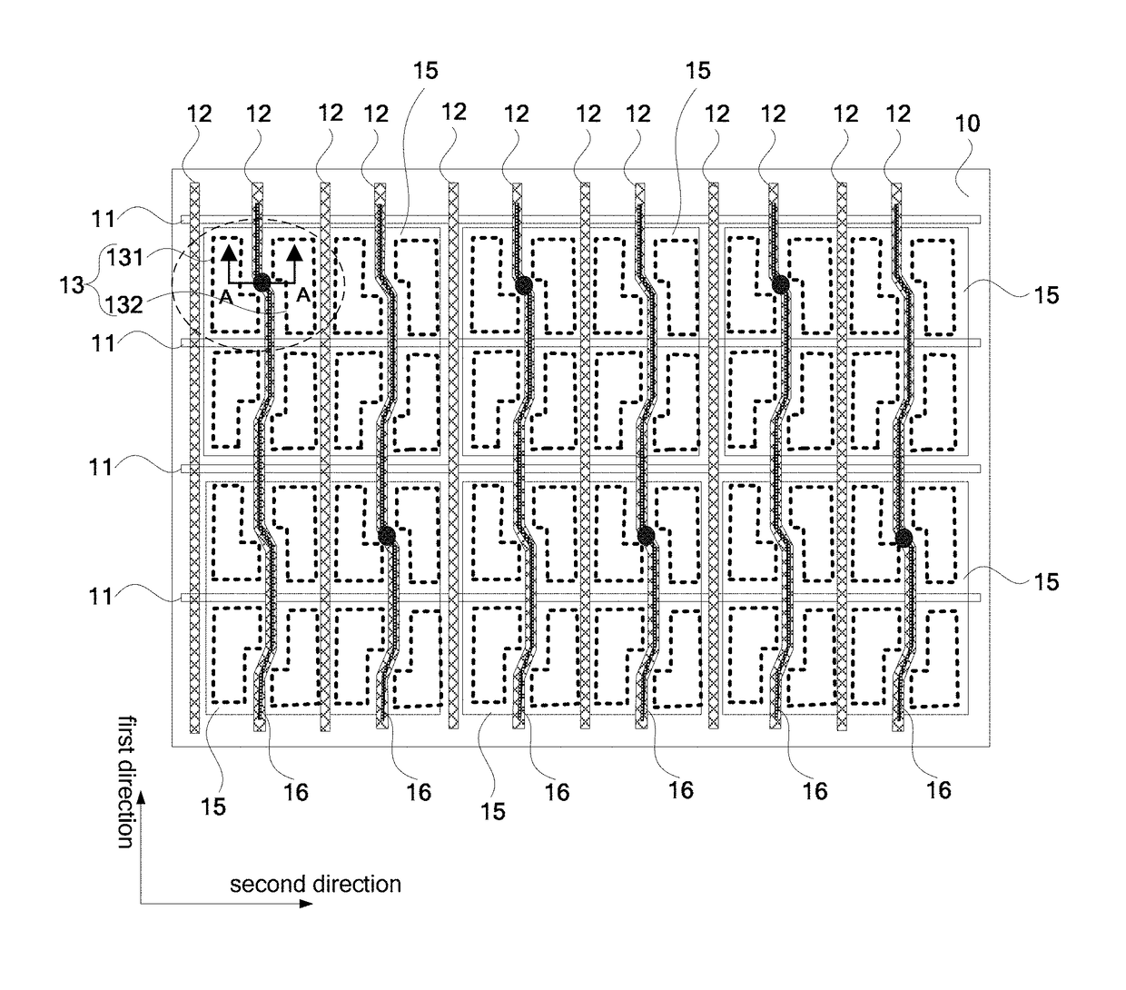
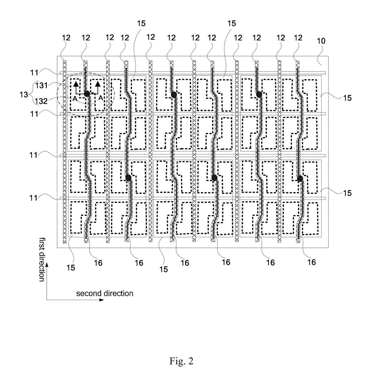
[0020]FIG. 2 is a top view showing a structure of a touch display panel provided by an embodiment. FIG. 3 is a partially enlarged view showing a pixel unit group in FIG. 2. As shown in FIG. 2 and FIG. 3, the touch display panel includes: a substrate 10, a plurality of scan lines 11 and a plurality of data lines 12, both of which are arranged at a first side of the substrate 10. As can be seen, the plurality of scan lines 11 are arranged in sequence, and the plurality of data lines 12 are arranged in sequence, and the scan lines 11 and the data ...


PUM


Abstract

The disclosure provides a touch display panel and a display device. The touch display panel includes a substrate, a plurality of scan lines, a plurality of data lines, pixel units, touch electrodes and a plurality of touch lines. Pixel electrodes in each pixel unit include a plurality of strip electrodes, and two adjacent pixel units form a unit group including a first pixel unit and a second pixel unit. The first pixel unit includes a first part and a second part. The second pixel unit includes a third part and a fourth part. The first pixel unit and the second pixel unit are in concave-convex fit arrangement. Each touch line is electrically connected to a corresponding touch electrode via a through hole located between the second part and the fourth part.

Description

CROSS-REFERENCES TO RELATED APPLICATIONS[0001]This application claims priority to Chinese Patent Application No. 201510946359.2, filed with the Chinese Patent Office on Dec. 16, 2015 and entitled “Touch Display panel and display device”, the contents of which are incorporated herein by reference in their entirety.TECHNICAL FIELD[0002]The present disclosure relates to the technical field of display, and in particular to a touch display panel and a display device.BACKGROUND[0003]With continuous evolution of intelligent mobile devices, requirements such as high resolution of pixel, light and thin structure, narrow frame and the like are expressed continuously. In order to enable display panels to be thinner and lighter, each display panel manufacturer explores integration of an external touch panel with a liquid crystal display panel. However, technology is complex and cost is high when manufacturing a component for integrating a touch panel with a liquid crystal panel under high resol...

Claims


Application Information

Patent Timeline
IPC IPC(8): G06F3/041G06F3/044
CPCG06F3/0418G06F2203/04111G06F3/0412G06F3/044G02F1/13338G02F1/134309G02F1/136227G06F3/0416G06F3/0443G06F3/0446
Inventor CAO, ZHAOKENGSONG, QIONGSHEN, POPING
Owner SHANGHAI TIANMA MICRO ELECTRONICS CO LTD
Features
  • Generate Ideas
  • Intellectual Property
  • Life Sciences
  • Materials
  • Tech Scout
  • Unparalleled Data Quality
  • Higher Quality Content
  • 60% Fewer Hallucinations
Learn More