Nitride based light emitting semiconductor device with desirable carbon to aluminum concentration ratio
- Summary
- Abstract
- Description
- Claims
- Application Information
AI Technical Summary
Benefits of technology
Problems solved by technology
Method used
Image
Examples
Embodiment Construction
[0022]Reference will now be made in detail to the present preferred embodiments of the invention, examples of which are illustrated in the accompanying drawings. Wherever possible, the same reference numbers are used in the drawings and the description to refer to the same or like parts.
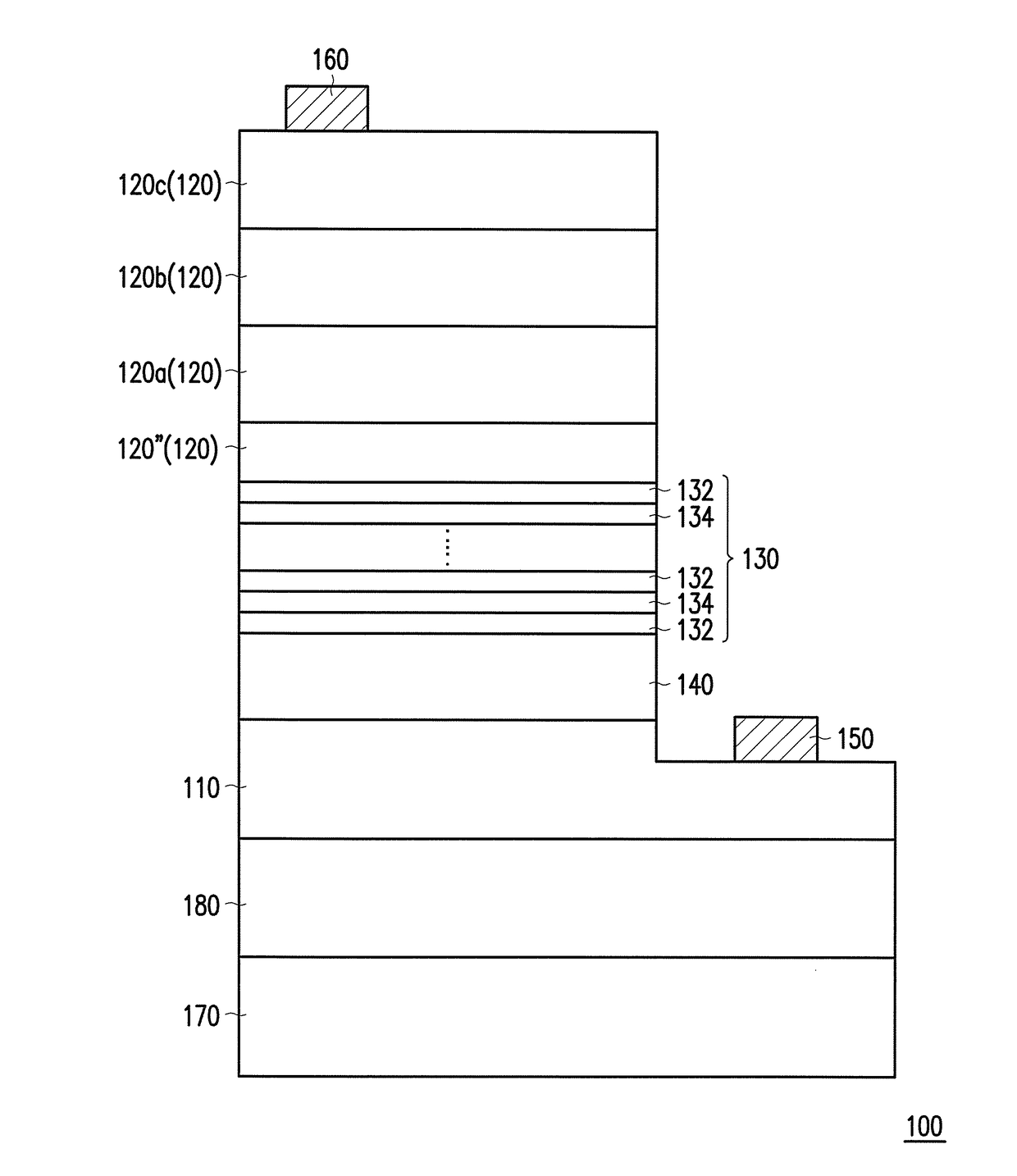
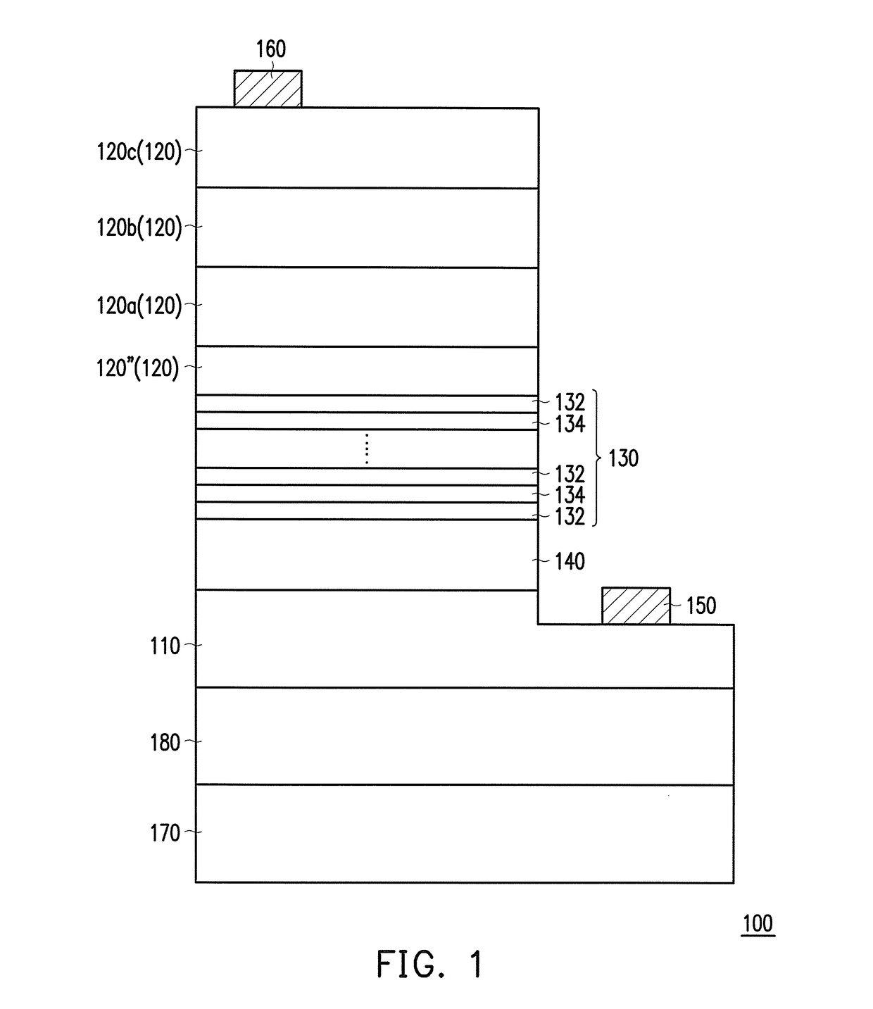
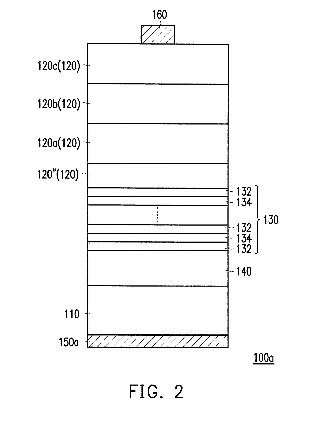
[0023]FIG. 1 is a schematic cross-sectional view of a semiconductor light-emitting device of an embodiment of the invention. Referring to FIG. 1, a semiconductor light-emitting device 100 of the embodiment includes at least one n-type semiconductor layer 110 (represented by one n-type semiconductor layer 110 as an example in FIG. 1), at least one p-type semiconductor layer 120 (represented by p-type semiconductor layers 120a, 120b, and 120c and an electron blocking layer 120″ as an example in FIG. 1), and a light-emitting layer 130. The light-emitting layer 130 is disposed between the p-type semiconductor layer 120 and the n-type semiconductor layer 110. In the embodiment, a material of the n-type se...
PUM
 Abstract
Description
Claims
Application Information


