Multijunction metamorphic solar cell for space applications

a solar cell and space technology, applied in the field of solar cells and the fabrication of solar cells, can solve the problems of complex interdependence and interaction, complex and often unpredictable ways, and the difficulty of properly specifying and manufacturing, and achieve the effect of increasing the efficiency of photoconversion

Active Publication Date: 2017-08-03
SOLAERO TECH CORP
View PDF0 Cites 15 Cited by
  • Summary
  • Abstract
  • Description
  • Claims
  • Application Information

AI Technical Summary

Benefits of technology

[0019]It is an object of the present disclosure to provide increased photoconversion efficiency in a multijunction solar cell for space applications over the operational life of the photovoltaic power system.

Problems solved by technology

Compared to silicon, III-V compound semiconductor multijunction devices have greater energy conversion efficiencies and generally more radiation resistance, although they tend to be more complex to properly specify and manufacture.
Such design variables are interdependent and interact in complex and often unpredictable ways.
In the terminology of some, such parameters are NOT simple “result effective” variables to those skilled in the art confronted with complex design specifications and practical operational considerations.

Method used


Image

  • Multijunction metamorphic solar cell for space applications
  • Multijunction metamorphic solar cell for space applications
  • Multijunction metamorphic solar cell for space applications

Examples


first embodiment

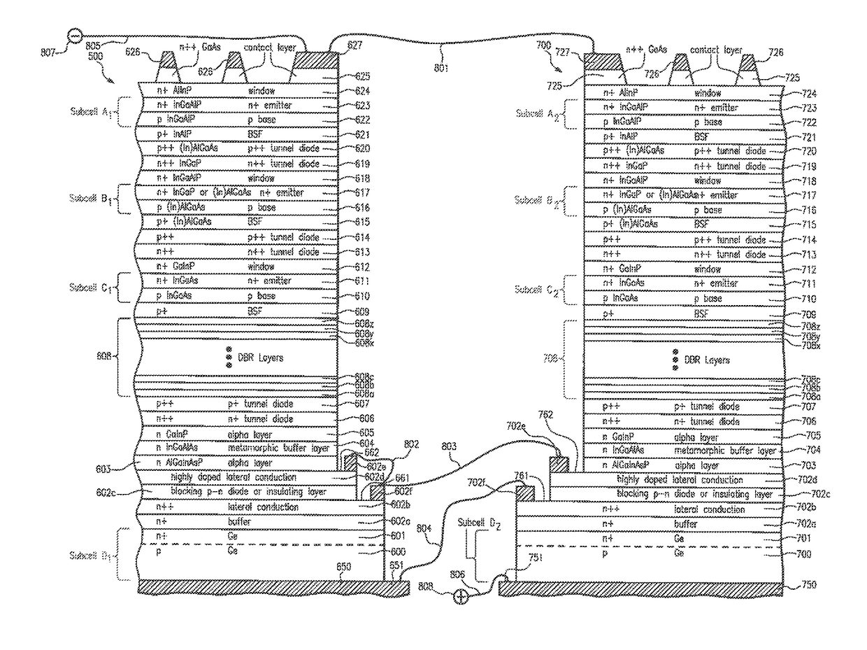
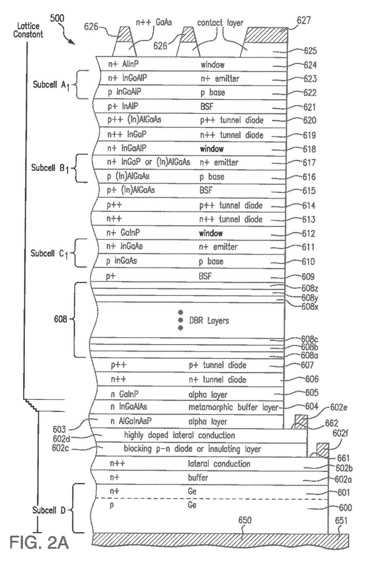
[0150]Turning to the fabrication of the multijunction solar cell assembly of the present disclosure, and in particular a five-junction solar cell assembly, FIG. 2A is a cross-sectional view of a four junction solar cell subassembly 500 after several stages of fabrication including the growth of certain semiconductor layers on the growth substrate, and formation of grids and contacts on the contact layer of the semiconductor body.

[0151]As shown in the illustrated example of FIG. 2A, the bottom subcell D1 includes a substrate 600 formed of p-type germanium (“Ge”) in some embodiments, which also serves as a base layer. A back metal contact pad 650 formed on the bottom of base layer 600 provides electrical contact 651 to the multijunction solar cell subassembly 500.

[0152]In some embodiments, the contact 651 may be in the interior of the region 600 and not on the bottom surface of the region 600.

[0153]In some embodiments, the bottom subcell D1 is germanium, while in other embodiments the...

second embodiment

[0194]the second solar cell subassembly similar to that of FIG. 2C is another configuration (not shown) with that the metamorphic buffer layer 604 is disposed above the tunnel diode layers 706, 707 and below the DBR layers 708 (not illustrated).

[0195]The foregoing multijunction solar cell subassemblies 500, 600, or 700 can be fabricated, for example, in wafer-level processes and then singulated or diced into individual semiconductor chips. The various semiconductor layers can be grown, one atop another, using known growth techniques (e.g., MOCVD) as discussed above.

[0196]Each solar cell subassembly 500, 600 and 700 also can include grid lines, interconnecting bus lines, and contact pads. The geometry and number of the grid lines, bus lines and / or contacts may vary in other implementations.

[0197]As previously mentioned, two (or more) solar cell subassemblies (e.g., 500 and 700) or chips can be disposed adjacent and parallel to one another and connected together electrically. For exam...


PUM


Abstract

A multijunction solar cell assembly and its method of manufacture including interconnected first and second discrete semiconductor body subassemblies disposed adjacent and parallel to each other, each semiconductor body subassembly including first top subcell, second (and possibly third) lattice matched middle subcells; a graded interlayer adjacent to the last middle solar subcell; and a bottom solar subcell adjacent to said graded interlayer being lattice mismatched with respect to the last middle solar subcell; wherein the interconnected subassemblies form at least a four junction solar cell by a series connection being formed between the bottom solar subcell in the first semiconductor body and the bottom solar subcell in the second semiconductor body.

Description

REFERENCE TO RELATED APPLICATIONS[0001]This application claims the benefit of U.S. Provisional Application No. 62 / 288,181 filed Jan. 16, 2016.[0002]The present application is related to U.S. patent application Ser. No. ______ filed simultaneously herewith.[0003]The present application is also related to U.S. Provisional Patent Application Ser. No. 62 / 243,239 filed Oct. 19, 2015.[0004]This application is also related to co-pending U.S. patent application Ser. No. 14 / 660,092 filed Mar. 17, 2015, which is a division of U.S. patent application Ser. No. 12 / 716,814 filed Mar. 3, 2010, now U.S. Pat. No. 9,018,521; which was a continuation in part of U.S. patent application Ser. No. 12 / 337,043 filed Dec. 17, 2008.[0005]This application is also related to co-pending U.S. patent application Ser. No. 13 / 872,663 filed Apr. 29, 2012, which was also a continuation-in-part of application Ser. No. 12 / 337,043, filed Dec. 17, 2008.[0006]This application is also related to co-pending U.S. patent appli...

Claims


Application Information

Patent Timeline
Patent Type & Authority Applications(United States)
IPC IPC(8): H01L31/02H01L31/05H01L31/054H01L31/18H01L31/0725H01L31/0735
CPCH01L31/02008H01L31/0725H01L31/0735H01L31/0547H01L31/1844H01L31/0504Y02E10/544H01L31/022425H01L31/06875H01L31/0693H01L31/078H01L31/1852Y02E10/52
Inventor DERKACS, DANIEL
Owner SOLAERO TECH CORP
Why Eureka
Try Eureka