Multijunction solar cells

a solar cell and multi-junction technology, applied in the field of solar cells and the fabrication of solar cells, can solve the problems of affecting the performance of solar cells, the occurrence of anomalous events in photovoltaic arrays, and the difficulty of properly specifying and manufacturing

Active Publication Date: 2022-08-04
SOLAERO TECH CORP
View PDF2 Cites 0 Cited by
  • Summary
  • Abstract
  • Description
  • Claims
  • Application Information

AI Technical Summary

Problems solved by technology

Compared to silicon, Ill-V compound semiconductor multijunction devices have greater energy conversion efficiencies and generally more radiation resistance, although they tend to be more complex to properly specify and manufacture.
Such rigorous testing and qualifications are not generally applicable to terrestrial solar cells and solar cell arrays.
The space solar cells and arrays experience a variety of complex environments in space missions, including the vastly different illumination levels and temperatures seen during normal earth orbiting missions, as well as even more challenging environments for deep space missions, operating at different distances from the sun, such as at 0.7, 1.0 and 3.0 AU (AU meaning astronomical units).
The photovoltaic arrays also endure anomalous events from space environmental conditions, and unforeseen environmental interactions during exploration missions.
Hence, electron and proton radiation exposure, collisions with space debris, and/or normal aging in the photovoltaic array and other systems could cause suboptimal operating conditions that degrade the overall power system performance, and may result in failures of one or more solar cells or array strings and consequent loss of power.
Such precautions are generally unnecessary in terrestrial applications.
In summary, it is evident that the differences in design, materials, and configurations between a space-qualified III-V compound semiconductor solar cell and subassemblies and arrays of such solar cells, on the one hand, and silicon solar cells or other photovoltaic devices used in terrestrial applications, on the other hand, are so substantial that prior teachings associated with silicon or other terrestrial photovoltaic system are simply unsuitable and have no applicability to the design configuration of space-qualified solar cells and arrays.
Charged particles in space could lead to damage to solar cell structures, and in some cases, dangerously high voltage being established across individual devices or conductors in the solar array.
These large voltages can lead to catastrophic electrostatic discharging (ESD) events.
However, in reality, changing a material parameter that increases the voltage may result in a decrease in current, and therefore a lower power output.
Such material design parameters are interdependent and interact in complex and often unpredictable ways, and for that reason are not “result ef...

Method used


Image

  • Multijunction solar cells
  • Multijunction solar cells
  • Multijunction solar cells

Examples


second embodiment

[0185]FIG. 1H is a and graph illustrating the band gap throughout the thickness of a solar subcell similar to that of FIG. 1B in a multijunction solar cell according to the present disclosure, in which the band gap is graded both in the emitter and base regions, in which in the emitter region it increases from the nominal band gap such as shown in FIG. 1A to a plateau at a higher band gap around the junction, and then decreases in the base region back down to the nominal band gap.

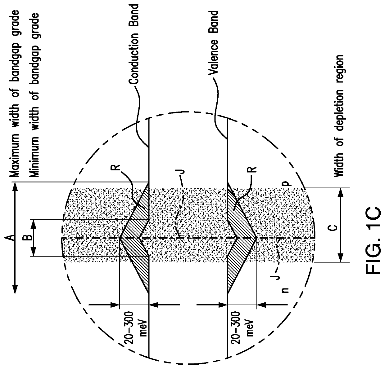
[0186]In some embodiments, the gradation in band gap increases to a certain level that is 20 meV to 300 meV greater than the nominal level, and then remains constant and plateaus at that level in the emitter region and continues at that level into the base regions symmetrically (or in other embodiments, non-symmetrically) around the junction. The gradation in band gap then decreases in the base region to the nominal band gap level as depicted in FIG. 1H.

third embodiment

[0187]FIG. 1I is a cross-sectional view and graph of the band gap throughout the thickness of a solar subcell in a multijunction solar cell according to the present disclosure, in which the band gap is graded in portions of both in the emitter and base layers, and in which in the emitter layer the band gap increases from the nominal band gap such as shown in FIG. 1A to a maximum value at the junction, and then decreases in the base layer back down to the nominal band gap in the portion of the base layer.

[0188]In this embodiment, the band gap in the emitter layer is flat or constant at a nominal value until a point where it begins increasing. The band gap then increases to a maximum value at the junction, and then decreases in the base layer back to the nominal value. However, unlike the embodiment in FIG. 1A, the band gap then increases in the base layer to a maximum value at the surface adjacent to the BSF layer.

[0189]In this embodiment, the increase in the band gap from the nomina...

fourth embodiment

[0190]FIG. 1J is a cross-sectional view and graph of the band gap throughout its thickness of a solar subcell in a multijunction solar cell according to the present disclosure, in which the band gap is graded in portions of both in the emitter and base layers, and in the emitter layer the band gap increases from the nominal band gap such as shown in FIG. 1A to a maximum value at the junction, and then decreases in the base layer back down to the nominal band gap in the portion of the base layer.

[0191]In this embodiment, the band gap in the emitter layer decreases from the surface of the emitter layer until a point where it stops at a nominal value and then begins increasing. The band gap then increases to a maximum value at the junction, and then decreases in the base layer back to the nominal value. As in the embodiment in FIG. 1L the band gap then increases in the base layer to a maximum value at the surface adjacent to the BSF layer.

[0192]In this embodiment, the decrease in the b...


PUM


Abstract

A multijunction solar cell including an upper first solar subcell having a first band gap and positioned for receiving an incoming light beam; a second solar subcell disposed below and adjacent to and lattice matched with said upper first solar subcell, and having a second band gap smaller than said first band gap; wherein at least one of the solar subcells has a graded band gap throughout the thickness of at least a portion of the active layer.

Description

REFERENCE TO RELATED APPLICATIONS[0001]This application is a continuation-in-part of U.S. patent application Ser. No. 17 / 161,314, filed Jan. 28, 2021.[0002]The present application is related to U.S. patent application Ser. No. 15 / 681,144 filed Aug. 18, 2017, which is a continuation-in-part of Ser. No. 14 / 828,206 filed Aug. 17, 2015.[0003]This application is related to U.S. patent application Ser. No. 14 / 660,092 filed Mar. 17, 2015, which is a division of U.S. patent application Ser. No. 12 / 716,814 filed Mar. 3, 2010, now U.S. Pat. No. 9,018,521; which is a continuation in part of U.S. patent application Ser. No. 12 / 337,043 filed Dec. 17, 2008.[0004]This application is also related to U.S. patent application Ser. No. 16 / 667,687 filed Oct. 29, 2019 which is a division of Ser. No. 13 / 872,663 filed Apr. 29, 2012, now U.S. Pat. No. 10,541,349, which was also a continuation-in-part of application Ser. No. 12 / 337,043, filed Dec. 17, 2008.[0005]This application is also related to U.S. paten...

Claims


Application Information

Patent Timeline
IPC IPC(8): H01L31/0687H01L31/0693
CPCH01L31/06875H01L31/0693H01L31/065H01L31/0687H01L31/0725H01L31/078Y02E10/544H01L31/0735
Inventor DERKACS, DANIELHART, JOHNBITTNER, ZACHARYESPENLAUB, ANDREW COLIN
Owner SOLAERO TECH CORP
Why Eureka
Try Eureka