Waveguide device, and antenna device including the waveguide device

Active Publication Date: 2017-08-17
WGR CO LTD +1
View PDF0 Cites 18 Cited by
  • Summary
  • Abstract
  • Description
  • Claims
  • Application Information

AI Technical Summary

Benefits of technology

[0017]According to an embodiment of the present disclosure, a recess exists in a side face at a branching portion of a waveguide member, such that the recess

Problems solved by technology

As such, a branching portion is susceptible to impedance mismatching, unless it is somehow remedied, and thus unwanted reflection of

Method used


Image

  • Waveguide device, and antenna device including the waveguide device
  • Waveguide device, and antenna device including the waveguide device
  • Waveguide device, and antenna device including the waveguide device

Examples


embodiment 1

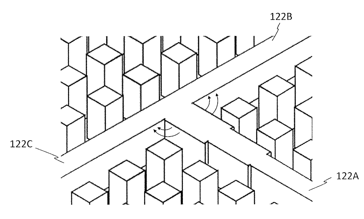
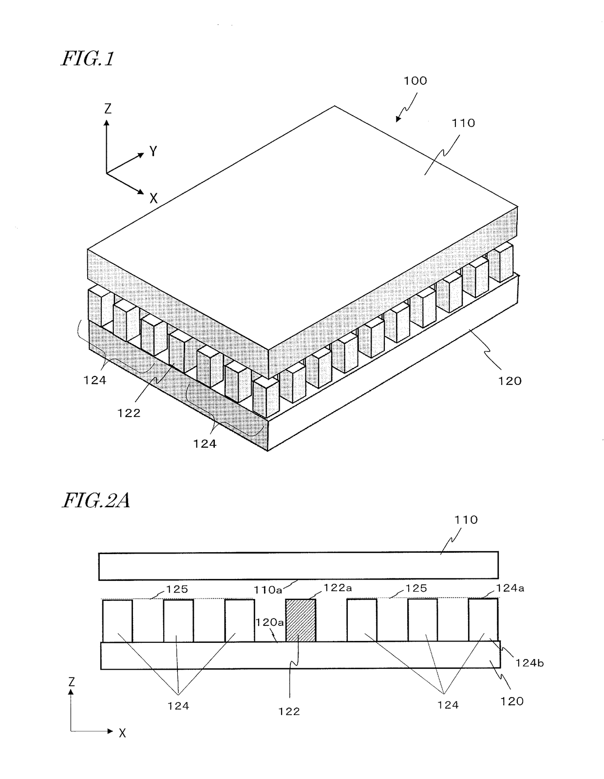
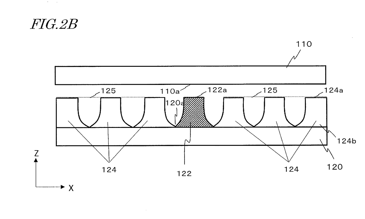
[0148]FIG. 12A is a perspective view schematically showing part of the structure of a waveguide device according to Embodiment 1 of the present disclosure. FIG. 12B is an upper plan view showing the waveguide device of FIG. 12A as viewed from the Z direction. FIG. 12A and FIG. 12B only show a portion close to a branching portion 136 of a waveguide member 122 in illustrative manners. In actuality, the conductive member 120, the waveguide member 122, and plural conductive rods 124 may also exist in the surroundings of the portion that is shown in the figure. This waveguide device further includes a conductive member 110 (see FIG. 1, etc.) covering over the waveguide member 122 and the plurality of conductive rods 124. The present embodiment differs in construction from the comparative example shown in FIG. 7 in that the waveguide member 122 has two recesses 137 in its side faces, near the branching portion 136.

[0149]Each of the second portion 122B and the third portion 122C of the wav...

embodiment 2

[0150]FIG. 13A is a perspective view schematically showing part of the structure of a waveguide device according to Embodiment 2 of the present disclosure. FIG. 13B is an upper plan view showing the waveguide device of FIG. 13A as viewed from the Z direction. In addition to the construction of Embodiment 1, impedance transformers are introduced in the first portion 122A of the waveguide member 122 according to the present embodiment. FIG. 13A and FIG. 13B only show a portion close to a branching portion 136 of a waveguide member 122 in illustrative manners. In actuality, the conductive member 120, the waveguide member 122, and plural conductive rods 124 may also exist in the surroundings of the portion that is shown in the figure. This waveguide device further includes a conductive member 110 (see FIG. 1, etc.) covering the waveguide member 122 and the plurality of conductive rods 124. The present embodiment differs in construction from the comparative example shown in FIG. 8A in th...

embodiment 3

[0161]FIG. 14A is a perspective view showing part of the structure of a waveguide device according to Embodiment 3 of the present disclosure. FIG. 14B is an upper plan view showing the structure of FIG. 14A as viewed from the Z direction. In the present embodiment, the impedance transformers 138A and 138B in the first portion 122A of the waveguide member 122 are realized by a structure with varying height, rather than width, of the waveguide face 122a. Moreover, on a side face opposite from the first portion 122A, the waveguide member 122 has a recess 139 at the junction (branching portion 136) where the first to third portions 122A to 122C are joined with one another, the recess 139 reaching the waveguide face 122a. In the present specification, the recess 137 in the second portion 122B of the waveguide member 122 may be referred to as a “first recess”, the recess 137 in the third portion 122C as a “second recess”, and the recess 139 in the branching portion 136 as a “third recess”...


PUM


Abstract

A waveguide device according to an embodiment includes an electrically conductive member having an electrically conductive surface, a waveguide member extending so as to face along the electrically conductive surface, and stretches of artificial magnetic conductor on both sides of the waveguide member. The waveguide member includes a first portion extending in one direction, and at least two branches extending in mutually different directions from one end of the first portion, the at least two branches including a second portion and a third portion. The second portion has a recess in a side face that connects to one side face of the first portion, the recess reaching the waveguide face.

Description

BACKGROUND[0001]1. Technical Field[0002]The present disclosure relates to a waveguide device, and an antenna device including the waveguide device.[0003]2. Description of the Related Art[0004]Examples of waveguiding structures including an artificial magnetic conductor are disclosed in Patent Documents 1 to 3 and Non-Patent Documents 1 to 3 as follows.[0005]Patent Document 1: International Publication No. 2010 / 050122[0006]Patent Document 2: the specification of U.S. Pat. No. 8,803,638[0007]Patent Document 3: the specification of European Patent Application Publication No. 1331688[0008]Non-Patent Document 1: H. Kirino and K. Ogawa, “A 76 GHz Multi-Layered Phased Array Antenna using a Non-Metal Contact Metamaterial Waveguide”, IEEE Transaction on Antenna and Propagation, Vol. 60, No. 2, pp. 840-853, February, 2012[0009]Non-Patent Document 2: A. Uz. Zaman and P.-S. Kildal, “Ku Band Linear Slot-Array in Ridge Gapwaveguide Technology, EUCAP 2013, 7th European Conference on Antenna and Pr...

Claims


Application Information

Patent Timeline
IPC IPC(8): H01Q13/24H01Q21/00
CPCH01Q21/0031H01Q13/24G01S7/02G01S13/931H01P3/123H01Q1/3233H01Q13/22
Inventor KIRINO, HIDEKIKAMO, HIROYUKI
Owner WGR CO LTD
Why Eureka
Try Eureka