Efficiently micro-transfer printing micro-scale devices onto large-format substrates

Active Publication Date: 2017-08-31
X DISPLAY CO TECH LTD
View PDF9 Cites 62 Cited by
  • Summary
  • Abstract
  • Description
  • Claims
  • Application Information

AI Technical Summary

Benefits of technology

[0024]Embodiments of the present invention enable the micro-transfer printing of spatially dense source devices from a relatively small source wafer to a spatially sparse arrangement o

Problems solved by technology

Because the source wafers are typically more expensive and smaller than the destination substrate and the spatial density of the source devices on the source wafer is much greater than the spatial density of the transferred source devices on the destination wafer, micro-transfer printing stamps transfer sparse arrays of source devices from the source wafer to the destination substrate.
Since many transfer

Method used


Image

  • Efficiently micro-transfer printing micro-scale devices onto large-format substrates
  • Efficiently micro-transfer printing micro-scale devices onto large-format substrates
  • Efficiently micro-transfer printing micro-scale devices onto large-format substrates

Examples


Embodiment Construction

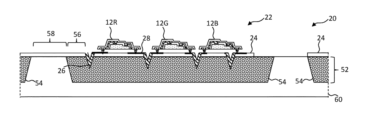
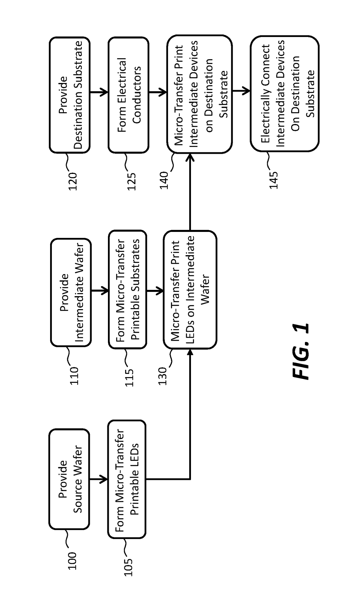
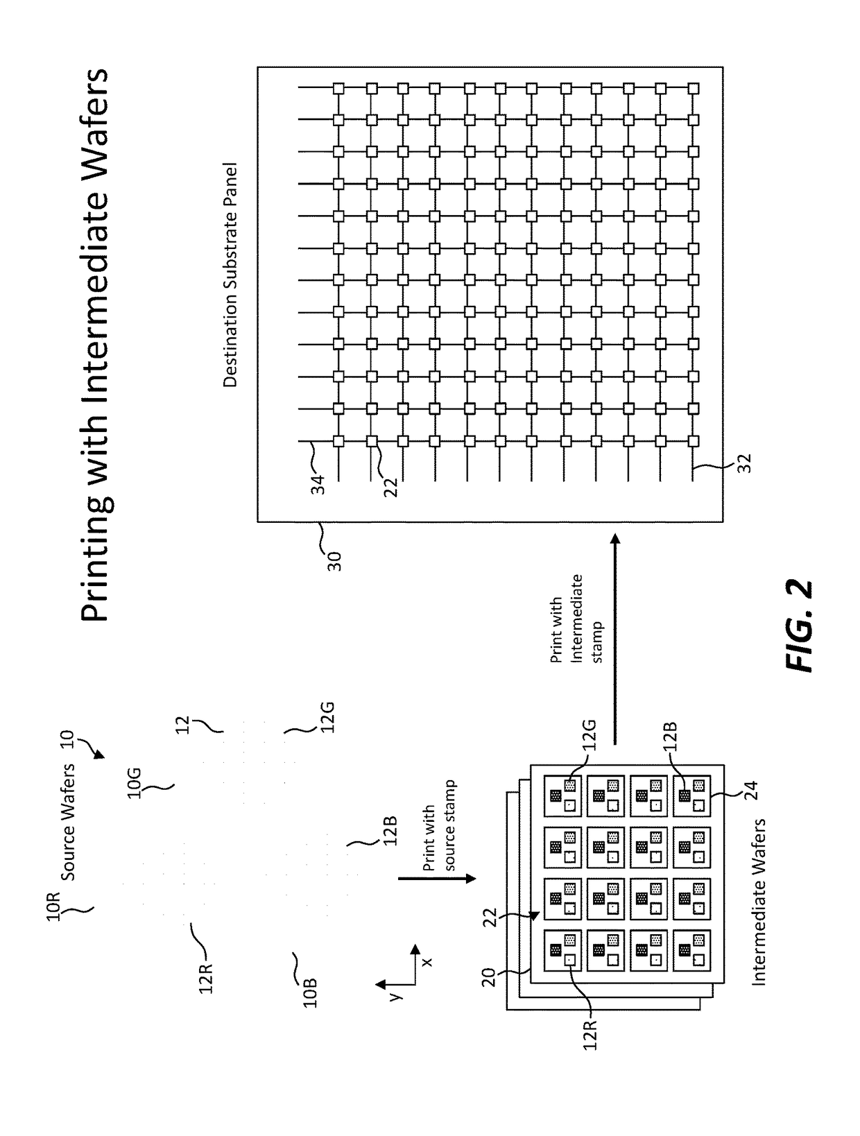
[0052]The present invention provides structures and methods for efficiently micro-transfer printing source devices from a source wafer to a destination substrate. Referring to the flow chart of FIG. 1 and the schematic illustration of FIG. 2, in an embodiment of the present invention a method of making a micro-transfer printed system or device includes providing a source wafer 10 in step 100. The source wafer 10 can be, for example, a semiconductor wafer or a compound semiconductor wafer. The source wafer 10 is provided in step 105 with a plurality of micro-transfer printable source devices 12 arranged in or on the source wafer 10 at a source spatial density. The source spatial density is the number of source devices 12 per unit area of the source wafer 10. The source devices 12 can be formed using integrated circuit photolithographic processes and, in certain embodiment, the source devices 12 are or include electronic elements such as light-emitting diodes (LEDs). In certain embodi...


PUM


Abstract

A method of making a micro-transfer printed system includes providing a source wafer having a plurality of micro-transfer printable source devices arranged at a source spatial density; providing an intermediate wafer having a plurality of micro-transfer printable intermediate supports arranged at an intermediate spatial density less than or equal to the source spatial density; providing a destination substrate; micro-transfer printing the source devices from the source wafer to the intermediate supports of the intermediate wafer with a source stamp having a plurality of posts at a source transfer density to make an intermediate device on each intermediate support; and micro-transfer printing the intermediate devices from the intermediate wafer to the destination substrate at a destination spatial density less than the source spatial density with an intermediate stamp having a plurality of posts at an intermediate transfer density less than the source transfer density.

Description

PRIORITY APPLICATION[0001]This application claims priority to and benefit of U.S. Patent Application No. 62 / 300,040, filed Feb. 25, 2016, entitled Efficiently Micro-Transfer Printing Micro-Scale Devices onto Large-Format Substrates, the content of which is hereby incorporated by reference.CROSS REFERENCE TO RELATED APPLICATION[0002]Reference is made to U.S. patent application Ser. No. 14 / 822,868, entitled Compound Micro-Assembly Strategies and Devices by Bower et al., the disclosure of which is incorporated herein by reference in its entirety.FIELD OF THE INVENTION[0003]The present invention relates to structures and methods for micro-transfer printing micro-scale devices from source wafers to large-format substrates.BACKGROUND OF THE INVENTION[0004]Substrates with electronically active components such as transistors or light-emitting diodes distributed over the extent of the substrate can be used in a variety of electronic systems, for example, flat-panel imaging devices such as fl...

Claims


Application Information

Patent Timeline
IPC IPC(8): H01L25/16H01L21/683H01L21/67H01L33/62H01L25/075
CPCH01L25/167H01L33/62H01L25/0753H01L2933/0066H01L21/6835H01L2221/68368H01L21/67144H01L2924/12044H01L24/97H01L2221/68354H01L2221/68381H01L2224/24227H01L2224/95136H01L2924/14H01L2924/1815H01L2924/18162H01L2924/12041H01L2224/82007H01L2224/951H01L33/0095
Inventor BOWER, CHRISTOPHERMEITL, MATTHEW
Owner X DISPLAY CO TECH LTD
Why Eureka
Try Eureka