Display apparatus and manufacturing method thereof

a technology of display apparatus and manufacturing method, which is applied in the direction of electrical apparatus, basic electric elements, and semiconductor devices, can solve the problems of high power consumption of tft-lcds, and low power efficiency of oleds, so as to reduce the rate at which final products in the manufacture of display apparatus are defective, improve display quality, and facilitate manufacturing

Active Publication Date: 2017-08-31
SEOUL SEMICONDUCTOR
View PDF3 Cites 62 Cited by
  • Summary
  • Abstract
  • Description
  • Claims
  • Application Information

AI Technical Summary

Benefits of technology

[0029]In addition, in various exemplary embodiments, the light emitting diode part is formed in a predetermined size such that a desired number of light emitting diodes parts can be coupled to TFT panel parts having various sizes. Thus, the display apparatus can be more conveniently manufactured in various sizes.
[0030]Furthermore, since the light emitting diode parts are constituted as a plurality of modules in some embodiments of the invention, any one of the light emitting diodes can be replaced by a new light emitting diode when the corresponding light emitting diode is defective, thereby providing a display apparatus having an improved display quality. Furthermore, since inspection of the light emitting diodes can be performed in a module unit in some embodiments of the invention, it is possible to reduce the rate at which final products in manufacture of the display apparatus are defective.

Problems solved by technology

As a result, the TFT-LCD suffers from constant power consumption regardless of brightness of a displayed screen.
On the other hand, although power consumption of an OLED has been continuously reduced due to the ongoing development of the technology, the OLED still has much higher power consumption than LEDs formed of inorganic semiconductors.
Thus OLEDs have low power efficiency.
Moreover, a passive matrix (PM) drive type OLED can suffer from deterioration in response speed upon pulse amplitude modulation (PAM) of the OLED having large capacitance, and can suffer from deterioration in lifespan upon high current driving through pulse width modulation (PWM) for realizing a low duty ratio.
Moreover, an AM driving type OLED requires connection of TFTs for each pixel, thereby causing increase in manufacturing costs and non-uniform brightness according to characteristics of TFTs.

Method used


Image

  • Display apparatus and manufacturing method thereof
  • Display apparatus and manufacturing method thereof
  • Display apparatus and manufacturing method thereof

Examples


first embodiment

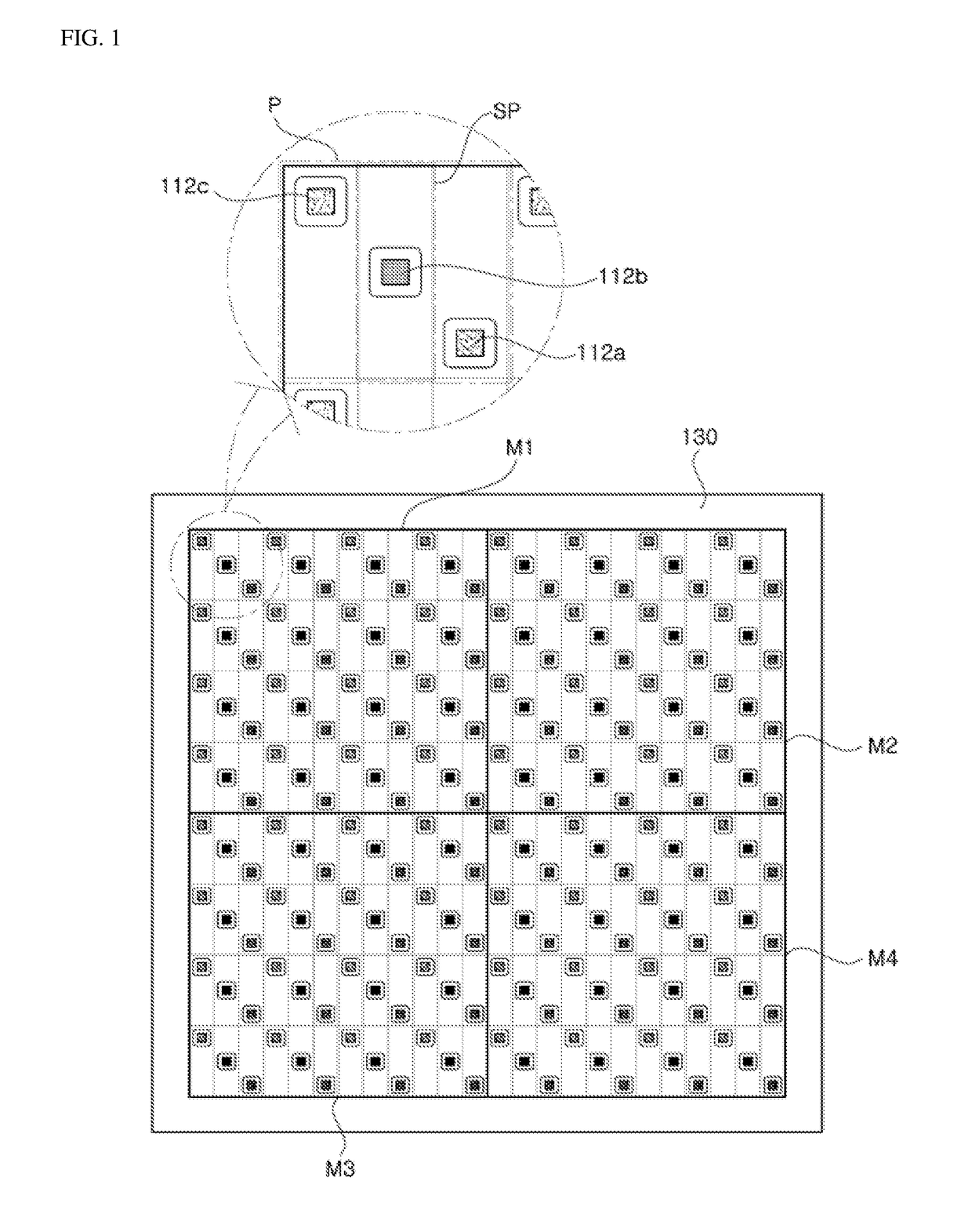
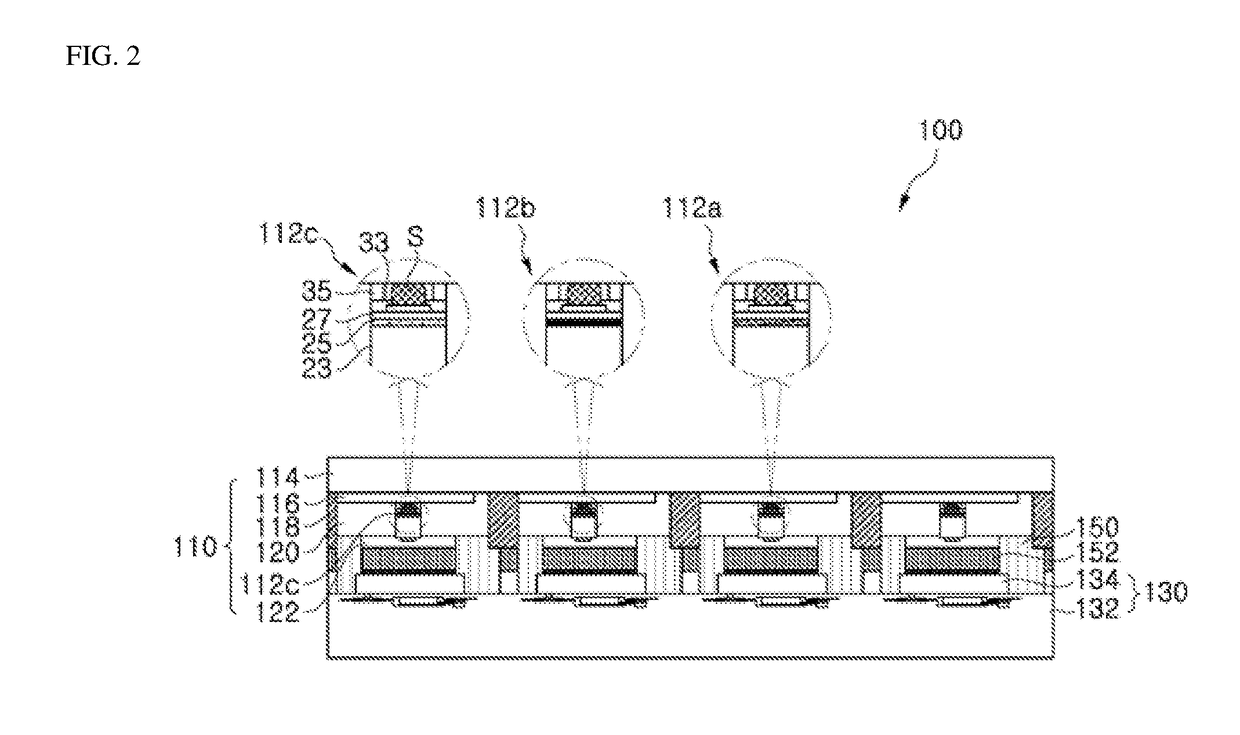
[0050]FIG. 1 is a plan view of a display apparatus constructed according to the principles of the invention. FIG. 2 is a cross sectional view of the display apparatus of FIG. 1.

[0051]Referring to FIG. 1 and FIG. 2, the display apparatus 100 according to the first exemplary embodiment includes a light emitting diode part 110, a TFT panel part 130, and an anisotropic conductive film 150.

[0052]The light emitting diode part 110 includes light emitting diodes 112, a support substrate 114, transparent electrodes 116, a blocking portion 118, an insulation layer 120, and is first connection electrodes 122. As shown in FIG. 2, in the light emitting diode part 110, the transparent electrode 116, the light emitting diode 112, the blocking portion 118, the insulation layer 120 and the first connection electrode 122 are formed in a generally vertical structure on the support substrate 114 to constitute one subpixel (SP) in the display apparatus 100, and the light emitting diode part 110 may be c...

second embodiment

[0078]FIG. 5 is a plan view of a display apparatus constructed according to the principles of the invention. FIG. 6 is a cross sectional view of the display apparatus of FIG. 5.

[0079]Referring to FIG. 5 and FIG. 6, the display apparatus 100 according to the second exemplary embodiment includes a light emitting diode part 110, a TFT panel part 130, and an anisotropic conductive film 150. The light emitting diode part 110 includes light emitting diodes, a support substrate 114, a transparent electrode 116, a blocking portion 118, an insulation layer 120, and first connection electrodes 122. The TFT panel part 130 includes a panel substrate 132 and second connection electrodes 134. Hereinafter, descriptions of the same components as previously described will be omitted to avoid redundancy.

[0080]In FIG. 5, blue light emitting diodes 112a are used as the light emitting diodes. Referring to FIG. 5, a plurality of blue light emitting diodes 112a is regularly arranged on the support substra...

third embodiment

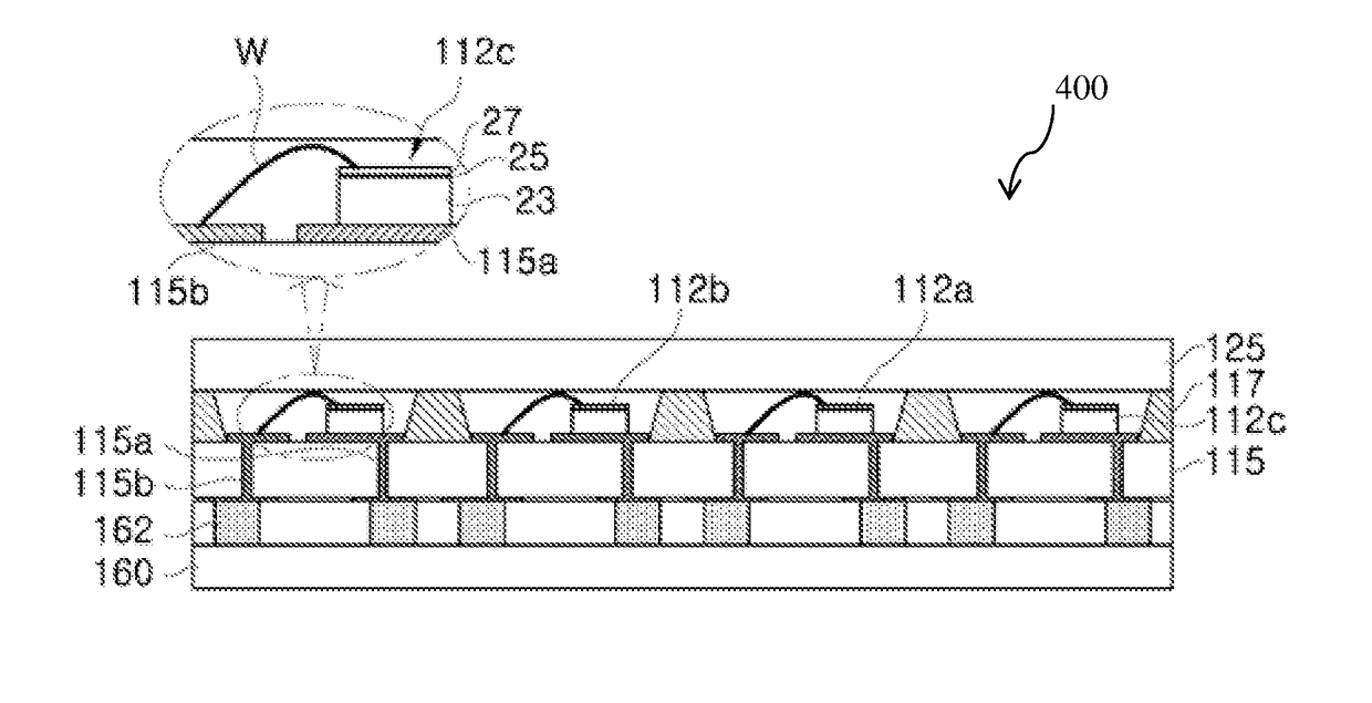
[0086]FIG. 7 is a cross sectional view of a display apparatus constructed according to the principles of the invention.

[0087]Referring to FIG. 7, the depicted display apparatus 100 includes a light emitting diode part 110 and a drive substrate 160. Descriptions of the same components as previously described will hereinafter be omitted to avoid redundancy.

[0088]The light emitting diode part 110 includes light emitting diodes 112, an electrode substrate 115 and a blocking portion 118, and may further include a protective substrate 128. As shown in FIG. 7, a plurality of the light emitting diodes 112 may be disposed on an upper surface of the electrode substrate 115 and the blocking portion 118 may be disposed between the light emitting diodes 112. Accordingly, a region formed by the blocking portion 118 may be each subpixel of the display apparatus 100.

[0089]The light emitting diode part 110 may include a plurality of light emitting diodes 112, which are regularly arranged on the elec...


PUM


Abstract

A display apparatus and a method of manufacturing the same includes a plurality of light emitting diode modules each including a plurality of light emitting diodes regularly arranged therein, and a substrate including a drive unit driving the plurality of light emitting diodes. The substrate is coupled to the plurality of light emitting diode modules such that they oppose each other; and, the drive unit is electrically connected to the plurality of light emitting diodes.

Description

CROSS-REFERENCE TO RELATED APPLICATIONS[0001]This application claims the benefit of U.S. Provisional Patent Application No. 62 / 300,249, filed on Feb. 26, 2016, and U.S. Provisional Patent Application No. 62 / 379,501, filed on Aug. 25, 2016, which are hereby incorporated by reference for all purposes as if fully set forth herein.BACKGROUND[0002]Field[0003]The invention relates generally to a display apparatus and a method of manufacturing the same, and, more particularly, to a display apparatus using micro-light emitting diodes and a method of manufacturing the same.[0004]Discussion of the Background[0005]A light emitting diode refers to an inorganic semiconductor device that emits light through recombination of electrons and holes. Light emitting diodes have been recently used in various fields including displays, automobile lamps, general lighting, and the like. A light emitting diode has various advantages such as long lifespan, low power consumption, and rapid response. As a resul...

Claims


Application Information

Patent Timeline
Patent Type & Authority Applications(United States)
IPC IPC(8): H01L33/62H01L33/50H01L27/12H01L27/15
CPCH01L33/62H01L27/153H01L33/502H01L2933/0066H01L27/1259H01L27/124H01L33/507H01L25/0753H01L33/504H01L2224/48091H01L2224/48227H01L2924/00014
Inventor TAKEYA, MOTONOBUKIM, YOUNG HYUNLEE, JONG IKOH, KWANG YONG
Owner SEOUL SEMICONDUCTOR
Why Eureka
Try Eureka