Display device and method of manufacturing a display device

a technology of display device and manufacturing method, which is applied in the direction of semiconductor devices, diodes, electrical devices, etc., can solve the problems of small interval between the pattern patterns of light-shielding film and the failure to obtain a shape as designed, and achieve the effect of reducing the luminan

Active Publication Date: 2017-08-31
JAPAN DISPLAY INC
View PDF0 Cites 11 Cited by
  • Summary
  • Abstract
  • Description
  • Claims
  • Application Information

AI Technical Summary

Benefits of technology

[0010]Even when the portions of different amounts of exposure are provided to form the concave and convex patterns in the picture-frame portion as in JP 2014-228723 A, the problem of failing to obtain a light-shielding film having a shape as designed occurs as the interval between the patterns of the light-shielding film becomes small. Moreover, when the light-shielding film is formed in multiple separate steps as in JP 2014-145924 A, the luminance is reduced if a shift occurs in the position of a photomask in each step.

Problems solved by technology

Even when the portions of different amounts of exposure are provided to form the concave and convex patterns in the picture-frame portion as in JP 2014-228723 A, the problem of failing to obtain a light-shielding film having a shape as designed occurs as the interval between the patterns of the light-shielding film becomes small.

Method used


Image

  • Display device and method of manufacturing a display device
  • Display device and method of manufacturing a display device
  • Display device and method of manufacturing a display device

Examples


first embodiment

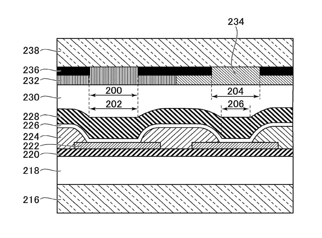
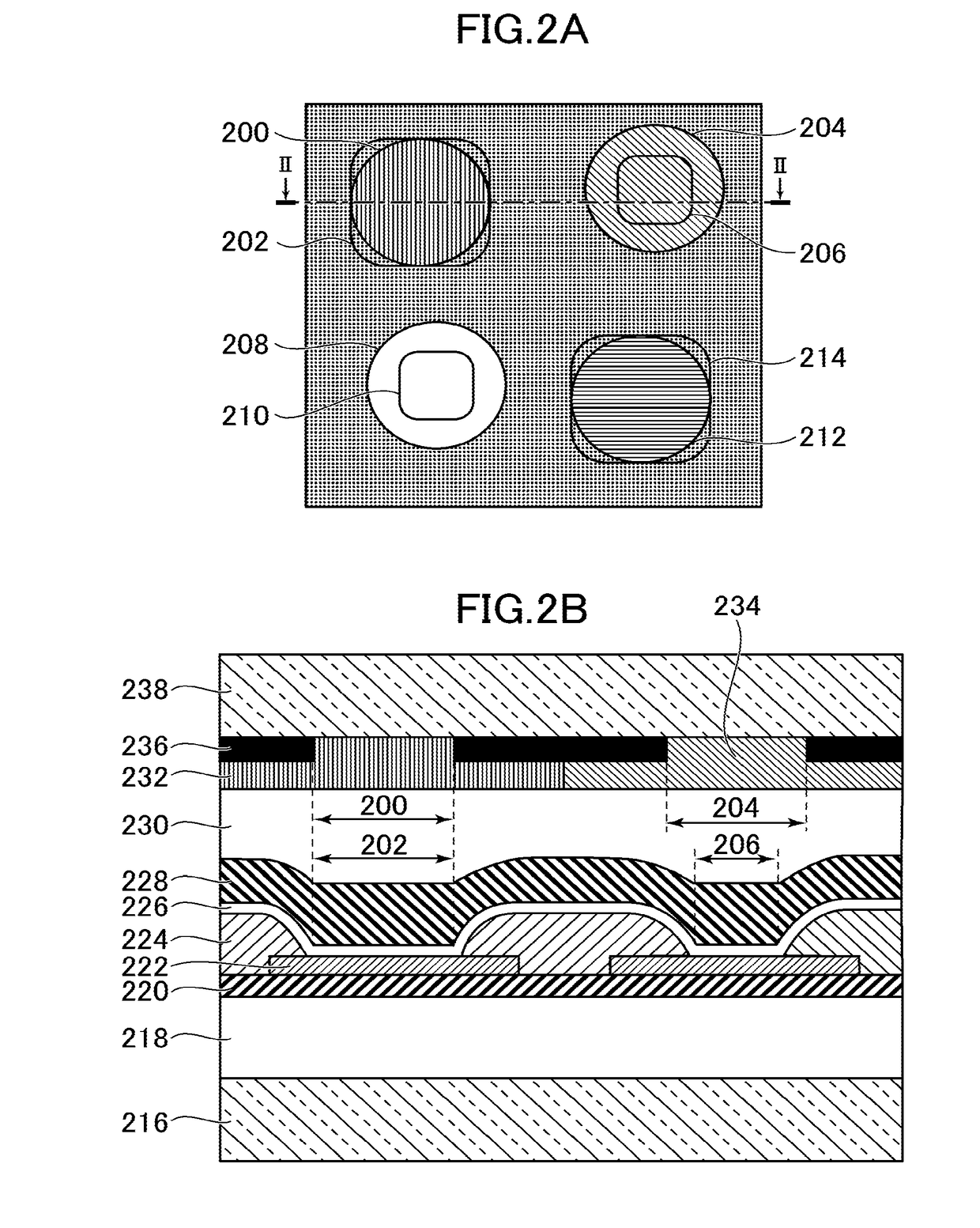
[0032]Subsequently, a first embodiment of the invention will be described. FIGS. 2A and 2B are respectively a plan view and a diagram showing a cross-section along line II-II in FIG. 2A in the first embodiment, both showing one pixel in an enlarged manner. As shown in FIG. 2A, a plurality of sub-pixels are disposed in two rows and two columns to constitute one pixel.

[0033]The sub-pixels include a first sub-pixel provided with a color filter that transmits light of a first color, and a second sub-pixel provided with a color filter that transmits light of a second color having a luminosity factor lower than that of the light of the first color. The first sub-pixel and the second sub-pixel are disposed adjacent to each other.

[0034]Specifically, the sub-pixels include a sub-pixel in which green or white light having a high luminosity factor is emitted, and a sub-pixel in which red or blue light having a low luminosity factor is emitted. On the drawing, a red sub-pixel that emits red lig...

second embodiment

[0057]Subsequently, a second embodiment of the invention will be described. FIGS. 5A and 5B are respectively a plan view and a diagram showing a cross-section along line V-V in FIG. 5A in the second embodiment, both showing one pixel in an enlarged manner. FIGS. 5A and 5B respectively correspond to FIGS. 2A and 2B in the first embodiment, and therefore, a description of configurations similar to those of the first embodiment is omitted.

[0058]The embodiment differs, compared to the first embodiment, in that the area of the transmission region provided in the first sub-pixel is formed smaller than the area of the light emission region provided in the first sub-pixel. Specifically, as shown in FIGS. 5A and 5B, the areas of the transmission regions 204 and 208 of the green sub-pixel and the white sub-pixel in the second substrate are formed smaller than the areas of the light emission regions 206 and 210 of the green sub-pixel and the white sub-pixel in the first substrate.

[0059]Similar...

third embodiment

[0064]Subsequently, a third embodiment of the invention will be described. FIGS. 7A and 7B are respectively a plan view and a diagram showing a cross-section along line VII-VII in FIG. 7A in the third embodiment, both showing one pixel in an enlarged manner. FIGS. 7A and 7B respectively correspond to FIGS. 2A and 2B in the first embodiment, and therefore, a description of configurations similar to those of the first embodiment is omitted.

[0065]The embodiment differs, compared to the first embodiment, in that the light-emitting layer included in the EL film 226 is formed not of a material that emits white light, but of materials that emit lights of different colors for the respective sub-pixels. Specifically, as shown in FIG. 7B, a red EL film 700 that emits red light is formed in the red sub-pixel, and a green EL film 702 that emits green light is formed in the green sub-pixel. When the light-emitting layer included in the EL film 226 is formed of the materials that emit lights of d...


PUM


Abstract

A display device includes a first substrate provided with a display region including a plurality of pixels arranged in a matrix, each of the plurality of pixels having a plurality of sub-pixels, and a second substrate provided with color filters and a light-shielding film, the color filters including transmission regions selectively transmitting lights of specific colors for the respective sub-pixels, the light-shielding film blocking light. The plurality of sub-pixels include a first sub-pixel provided with the transmission region that transmits light of a first color, and a second sub-pixel provided with the transmission region that transmits light of a second color having a luminosity factor lower than that of the light of the first color. A difference in area between a light-emitting region and the transmission region in the second sub-pixel is smaller than a difference in area between a light-emitting region and the transmission region in the first sub-pixel.

Description

CROSS-REFERENCE TO RELATED APPLICATION[0001]The present application claims priority from the Japanese Application JP2016-37915 filed on Feb. 29, 2016, the content of which is hereby incorporated by reference into this application.BACKGROUND OF THE INVENTION[0002]1. Field of the Invention[0003]The present invention relates to a display device and a method of manufacturing a display device.[0004]2. Description of the Related Art[0005]In recent years, a thin display device such as an organic EL display device or a liquid crystal display device has remarkably developed, because of its features such as thinness, light weight, and low power consumption, as a possible substitute for a CRT, which had conventionally been in the mainstream of display devices. Especially a high resolution of a display image has developed, which requires the technique for manufacturing a color filter suitable for a display device having a high resolution.[0006]The size of one pixel is reduced as the resolution ...

Claims


Application Information

Patent Timeline
Patent Type & Authority Applications(United States)
IPC IPC(8): H01L51/52H01L27/32
CPCH01L51/5284H01L27/3216H01L27/3213H01L27/322H10K59/351H10K59/352H10K59/38H10K50/865
Inventor TOKUDA, NAOKI
Owner JAPAN DISPLAY INC
Why Eureka
Try Eureka