Method for forming fin structures for non-planar semiconductor device

a semiconductor device and fin structure technology, applied in the direction of semiconductor devices, electrical equipment, basic electric elements, etc., can solve the problems of silicon loss during fabrication processing

Active Publication Date: 2017-09-14
UNITED MICROELECTRONICS CORP
View PDF0 Cites 12 Cited by
  • Summary
  • Abstract
  • Description
  • Claims
  • Application Information

AI Technical Summary

Benefits of technology

[0009]According to the method for forming fin structures provide by the present invention, the fin width of the first fin is made larger than the fin width of the second fins because the spacing width between the first fin and the second fins is larger than the spacing width between the second fins. More important, since the

Problems solved by technology

More important, since the second fins are removed, the first fin is taken as positioned in an iso region and thus suffers silicon loss during fabrication processing.
However, b

Method used


Image

  • Method for forming fin structures for non-planar semiconductor device
  • Method for forming fin structures for non-planar semiconductor device
  • Method for forming fin structures for non-planar semiconductor device

Examples


Embodiment Construction

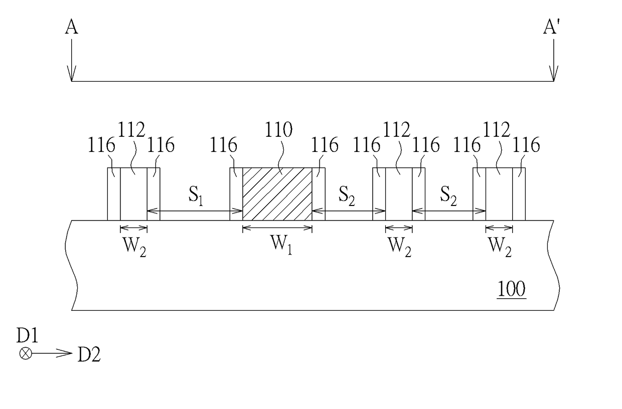
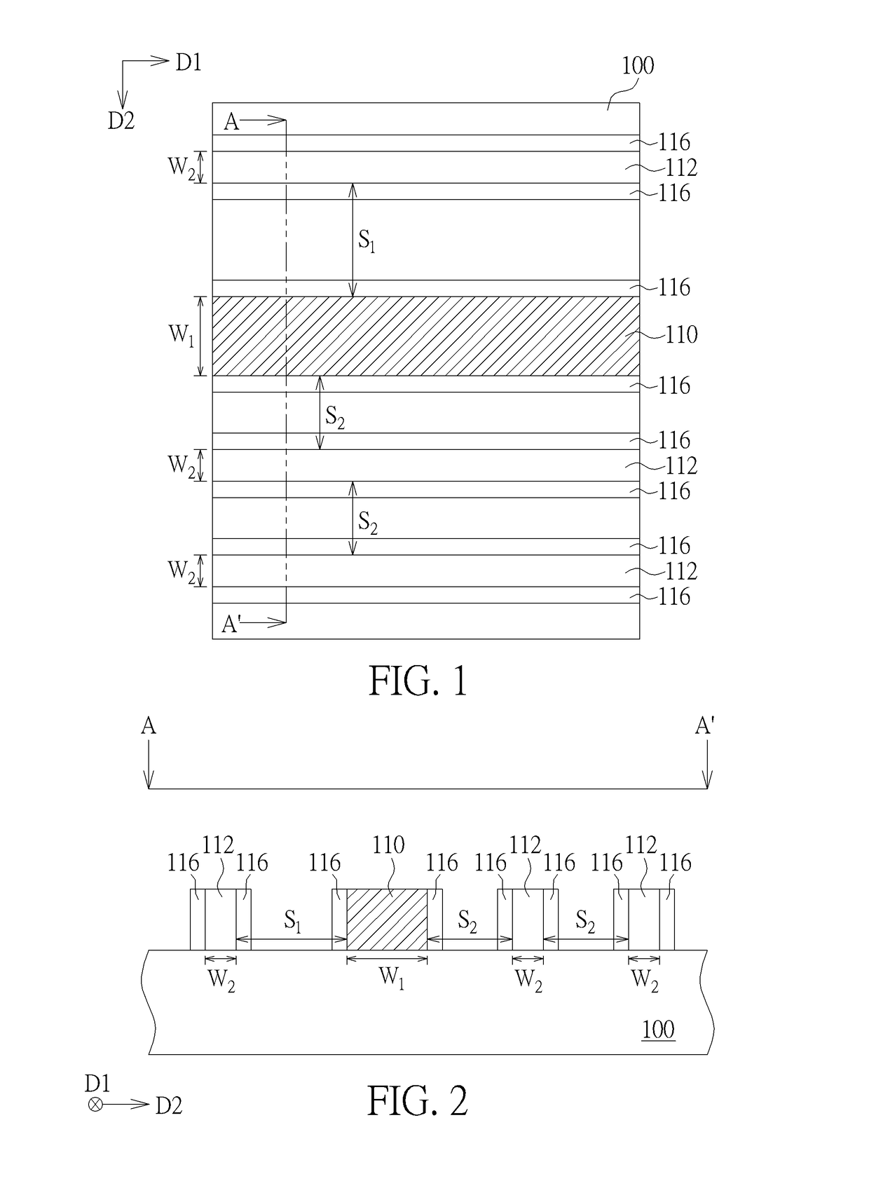
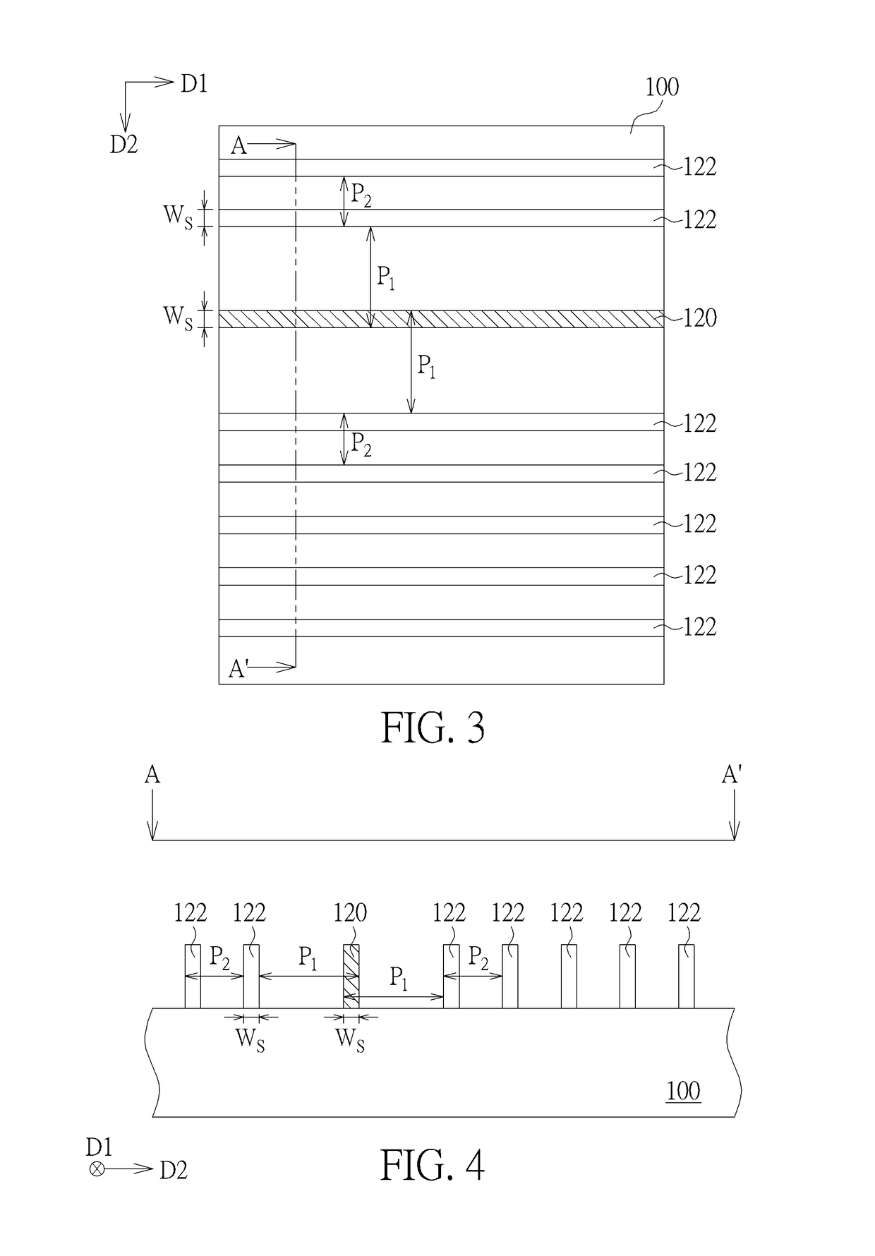
[0027]In the following description, numerous specific details are set forth, such as particular structures, components, materials, dimensions, processing steps and techniques, in order to provide a thorough understanding of the present invention. However, it will be appreciated by one of ordinary skill in the art that the invention maybe practiced without these specific details. In other instances, well-known structures or processing steps have been described in detail in order to avoid obscuring the invention.

[0028]It will be understood that when an element is referred to as being “formed” on another element, it can be directly or indirectly, formed on the given element by growth, deposition, etch, attach, connect, or couple. And it will be understood that when an elements or a layer is referred to as being “on”, “connected to”, or “coupled to” another element or layer, it can be directly on, connected or coupled to the other element or layer or intervening elements or layers may b...


PUM


Abstract

A method for forming fin structure includes following steps. A substrate is provided. A first mandrel and a plurality of second mandrels are formed on the substrate simultaneously. A plurality of spacers are respectively formed on sidewalls of the first mandrel and the second mandrels and followed by removing the first mandrel and the second mandrels to form a first spacer pattern and a plurality of second spacer patterns. Then the substrate is etched to simultaneously form at least a first fin and a plurality of second fins on the substrate with the first spacer pattern and the second spacer patterns serving as an etching mask. At least one of the second fins is immediately next to the first fin, and a fin width of the first fin is larger than a fin width of the second fins. Then, the second fins are removed from the substrate.

Description

BACKGROUND OF THE INVENTION[0001]1. Field of the Invention[0002]The present invention relates to a method for forming fin structures for non-planar semiconductor device, and more particularly, to a method for forming fin structures for non-planar semiconductor device using sidewall image transfer (hereinafter abbreviated as SIT) technique.[0003]2. Description of the Prior Art[0004]Conventional planar metal-oxide-semiconductor (MOS) transistor has difficulty when scaling down to 65 nm and below. Therefore the non-planar transistor technology such as Fin Field effect transistor (FinFET) technology that allows smaller size and higher performance is developed to replace the planar MOS transistor.[0005]The FinFET device is conventionally formed by: First a silicon layer of a substrate is patterned to form fin structures (not shown) by a proper etching process. Then, an insulating layer surrounding lower portions of the fin structures is formed and followed by forming a gate covering a po...

Claims


Application Information

Patent Timeline
IPC IPC(8): H01L21/033H01L21/8234
CPCH01L21/823431H01L21/0337H01L21/845H01L29/6681
Inventor LI, KUAN-HSIENHUANG, RAI-MINTSENG, I-MINGLIANG, WEN-ANHUANG, CHEN-MING
Owner UNITED MICROELECTRONICS CORP
Why Eureka
Try Eureka