

Display device
- Summary
- Abstract
- Description
- Claims
- Application Information
AI Technical Summary
Benefits of technology
Problems solved by technology
Method used
Image

Examples
first embodiment
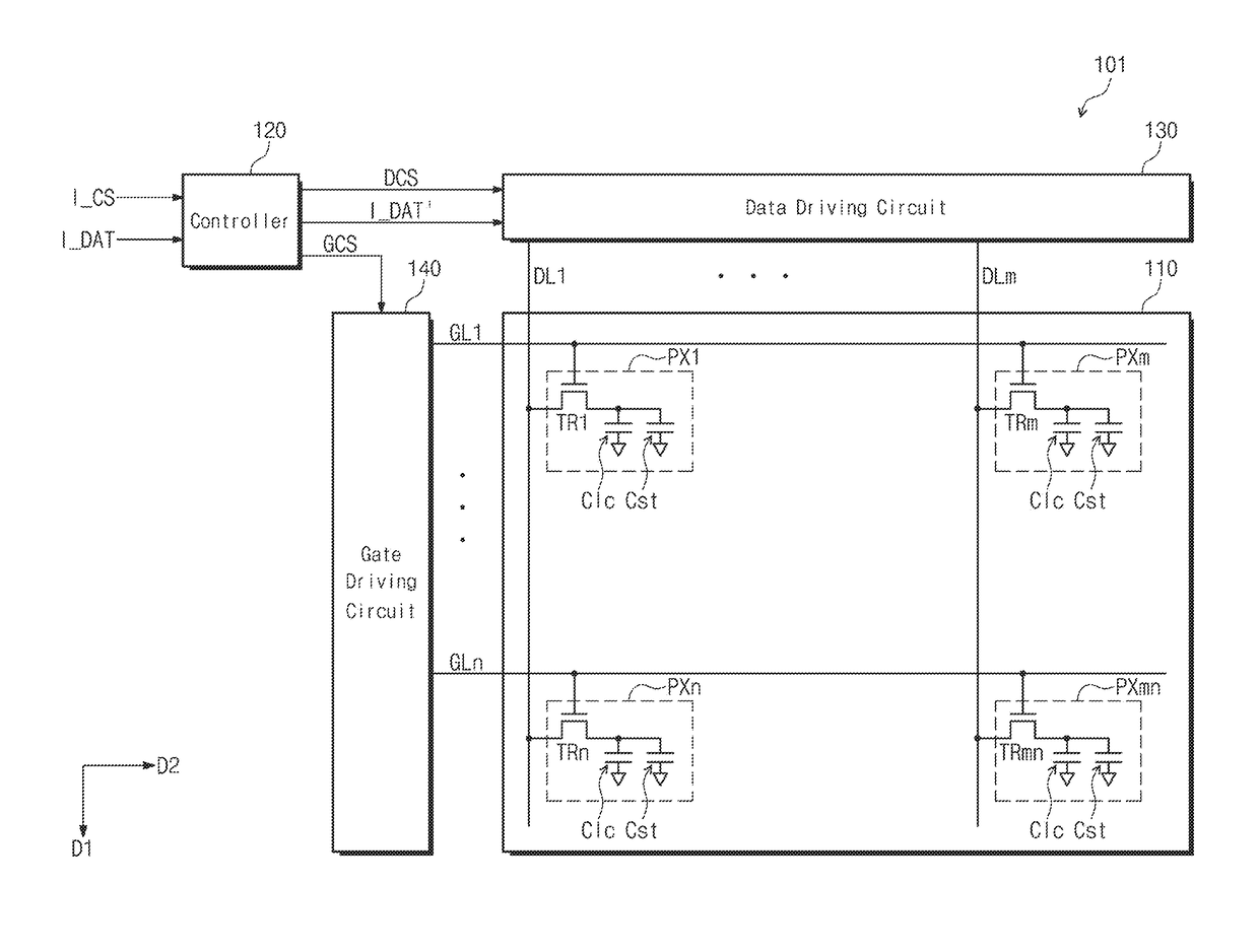
[0057]FIG. 1 is a plan view of a display device constructed according to the principles of the invention illustrating the size of the drain electrodes of the pixels decreasing along a data line.
[0058]Referring to FIG. 1, a display device 101 includes a display panel 110, a controller 120, a data driving circuit 130, and a gate driving circuit 140.
[0059]The display panel 110 includes a plurality of data lines DL1 to DLm, a plurality of gate lines GL1 to GLn, and a plurality of thin film transistors TR1 to TRmn.
[0060]The plurality of data lines DL1 to DLm extend in a first direction D1 and the plurality of gate lines GL1 to GLn extend in a second direction D2 intersecting the first direction D1. The plurality of thin film transistors TR1 to TRmn are connected to the plurality of data lines DL1 to DLm and the plurality of gate lines GL1 to GLn. In one or more exemplary embodiments, when the plurality of data lines DL1 to DLm are provided in m columns and the plurality of gate lines GL1...
second embodiment
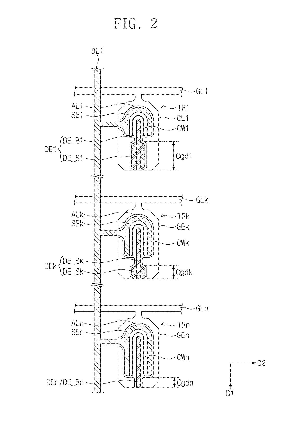
[0098]FIG. 5 is a plan view of display device constructed according to the principles of the invention illustrating the size of the overlapping area between the drain electrode and storage capacitor of the pixels increasing along a data line. In FIG. 5, the same reference numerals as those in FIG. 2 refer to the same components and their overlapping descriptions will be omitted to avoid redundancy.
[0099]Referring to FIG. 5, in order to compensate for the delay of the data signal, the channel width of each of the plurality of thin film transistors TR1 to TRn connected to the first data line DL1 increases as the distance between a corresponding thin film transistor and the data driving circuit 130 increases. This is identical to that of the embodiment of FIG. 2.
[0100]If the channel width of each of the plurality of thin film transistors TR1 to TRn varies according to the distance from the data driving circuit 130, a deviation of the kickback voltage Vkb results between the plurality o...
third embodiment
[0112]FIG. 6 is a plan view of display device constructed according to the principles of the invention illustrating thin film transistors having I-shaped channels connected to a first data line.
[0113]Referring to FIG. 6, the plurality of thin film transistors TR1 to TRn are connected to the first data line DL1 along the first direction D1FIG. 6 illustrates that each of the plurality of thin film transistors TR1 to TRn has an I-shaped channel structure. Additionally, FIG. 6 illustrates only the first, kth, and nth thin film transistors TR1, TRk, and TRn of the plurality of thin film transistors TR1 to TRn, connected to a first gate line GL1, a kth gate line GLk, and an nth gate line GLn.
[0114]In order to compensate for the delay of the data signal, the channel width of each of the plurality of thin film transistors TR1 to TRn connected to the first data line DL1 increases as the distance between a corresponding thin film transistor and the data driving circuit 130 increases. Accordin...
PUM
 Abstract
Description
Claims
Application Information