Switching circuit and high frequency module
a high-frequency module and switching circuit technology, applied in electronic switching, pulse technique, semiconductor/solid-state device details, etc., can solve the problems of reducing the size of the circuit, unable to obtain desired transmission characteristics, and difficulty in obtaining sufficient isolation between the communication system, so as to achieve effective attenuation of unnecessary signals and improve isolation characteristics
- Summary
- Abstract
- Description
- Claims
- Application Information
AI Technical Summary
Benefits of technology
Problems solved by technology
Method used
Image
Examples
first preferred embodiment
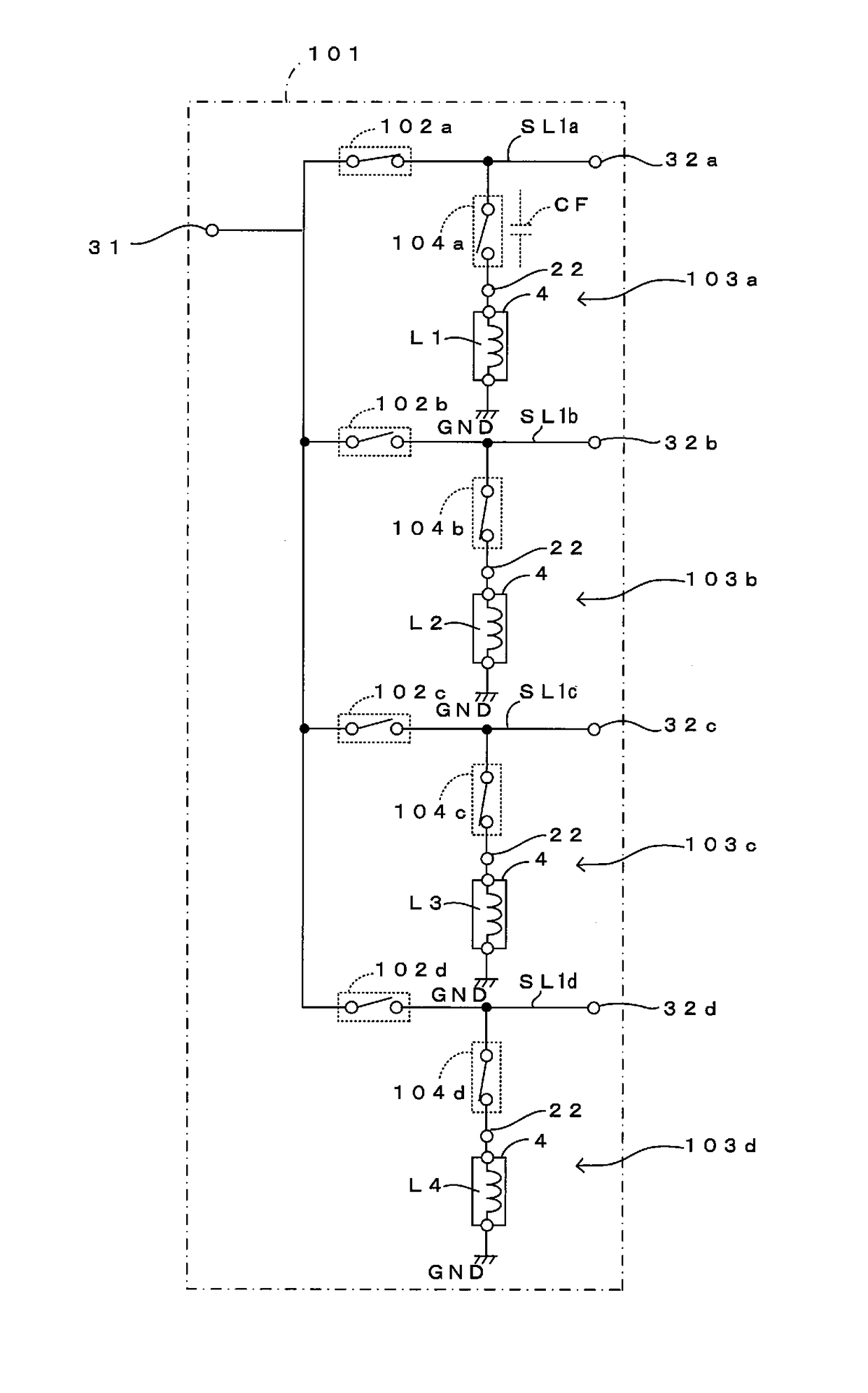
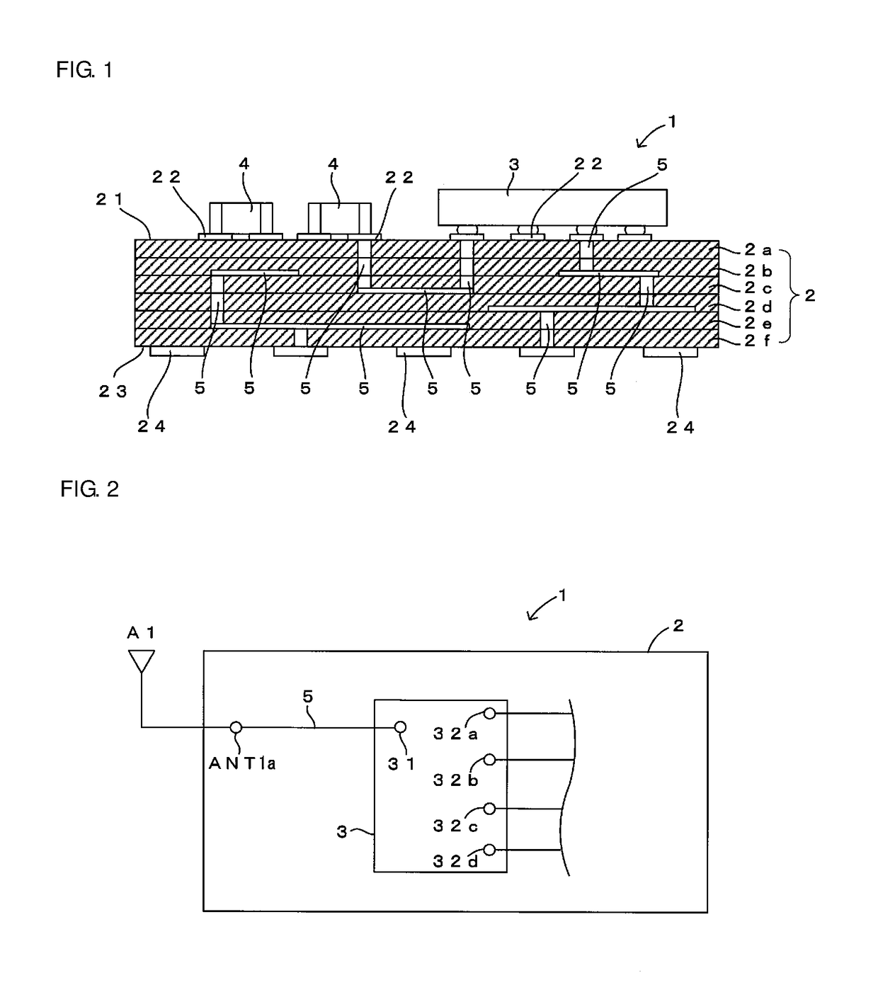
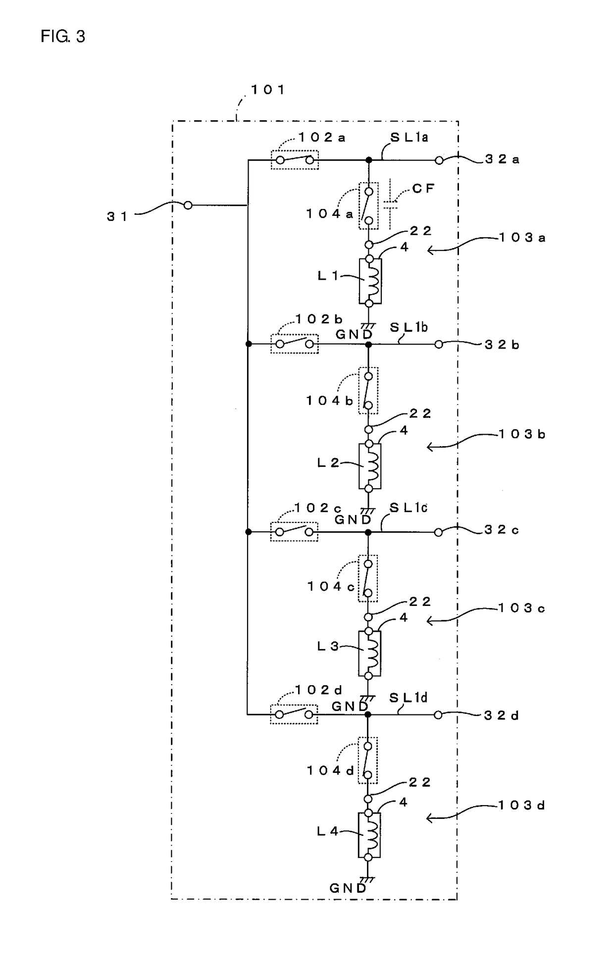
[0032]A first preferred embodiment of the present invention will be described with reference to FIGS. 1 to 4. FIGS. 1 to 3 illustrate only a main configuration according to a preferred embodiment of the present invention. To simplify the description, the other configurations are not illustrated. Similarly to FIGS. 1 to 3, FIGS. 6 and 7 referred to in the description below also illustrate only a main configuration, and will not be described in the description thereof below.
[0033]A high frequency module 1 illustrated in FIGS. 1 and 2 is preferably mounted in a communication device (not illustrated) such as a cellular phone supporting the multi-mode and multi-bands in which multiple frequency bands are used to perform communication. Such a communication device supports multiple communication systems, such as the GSM standard, the W-CDMA standard, the LTE standard, and the Bluetooth standard. The high frequency module 1 includes a switching circuit that couples, through switching, an an...
second preferred embodiment
[0046]Referring to FIGS. 6 and 7, a second preferred embodiment of the present invention will be described. The high frequency module 1 according to this preferred embodiment is different from that according to the first preferred embodiment described above in that, as illustrated in FIG. 6, a common terminal 33 (corresponding to a “third terminal” of the present invention) coupled to an antenna A2 is further included in a switch IC 3a. In the description below, points different from those in the first preferred embodiment will be mainly described. The other configurations and operations are similar to those in the first preferred embodiment described above, and are designated with identical reference characters. Thus, the other configurations and operations will not be described.
[0047]As illustrated in FIG. 6, the switch IC 3a includes the common terminal 31 coupled to a common electrode ANT1 (external connecting terminal 24) through a wiring electrode 5, the common terminal 33 cou...
PUM
 Abstract
Description
Claims
Application Information


