Micro-led element for horizontally-aligned assembly, method for manufacturing same, and horizontally-aligned assembly comprising same

a technology of led elements and assembly, which is applied in the direction of nanostructure manufacturing, lighting and heating apparatus, and nanostructure assembly, etc., can solve the problems of nano- or micro-scale devices, the method of mounting nano-scale led elements on electrodes, and the inability to individually arrange and mount nano-scale led elements in the target electrode region. , to achieve the effect of improving the alignment of the mounted element, improving the number of led elements, and easy assembly

Active Publication Date: 2017-11-02
SAMSUNG DISPLAY CO LTD
View PDF16 Cites 31 Cited by
  • Summary
  • Abstract
  • Description
  • Claims
  • Application Information

AI Technical Summary

Benefits of technology

[0032]The present invention can implement a nano-scale light-emitting diode (LED) element that can be easily laid in a length direction and mounted on a desired electrode region to improve an alignment of the mounted element. As a result, it is possible to significantly increase the number of LED elements that are included per unit area of an electrode line and significantly improve electrical connectivity between the electrode and the LED elements. The present invention can also implement a horizontal array assembly that can significantly increase the number of nano-

Problems solved by technology

In particular, methods of mounting nano-scale LED elements on electrodes still have difficulties in that it is very difficult to place and mount nano-scale LED elements on electrodes as intended because of a limitation of a size of each of the nano-scale LED elements.
This is because nano-scale LED elements are nano- or micro-scale devices and cannot be individually arranged and mounted in a target electrode region with human hands.
In addition, it is very difficult to control the number of nano-scale LED elements included in a unit electrode region, a posit

Method used


Image

  • Micro-led element for horizontally-aligned assembly, method for manufacturing same, and horizontally-aligned assembly comprising same
  • Micro-led element for horizontally-aligned assembly, method for manufacturing same, and horizontally-aligned assembly comprising same
  • Micro-led element for horizontally-aligned assembly, method for manufacturing same, and horizontally-aligned assembly comprising same

Examples


Embodiment Construction

Technical Problem

[0008]The present invention is designed to solve the above problems.

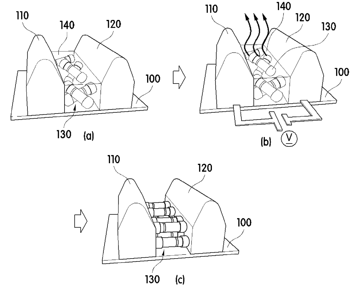
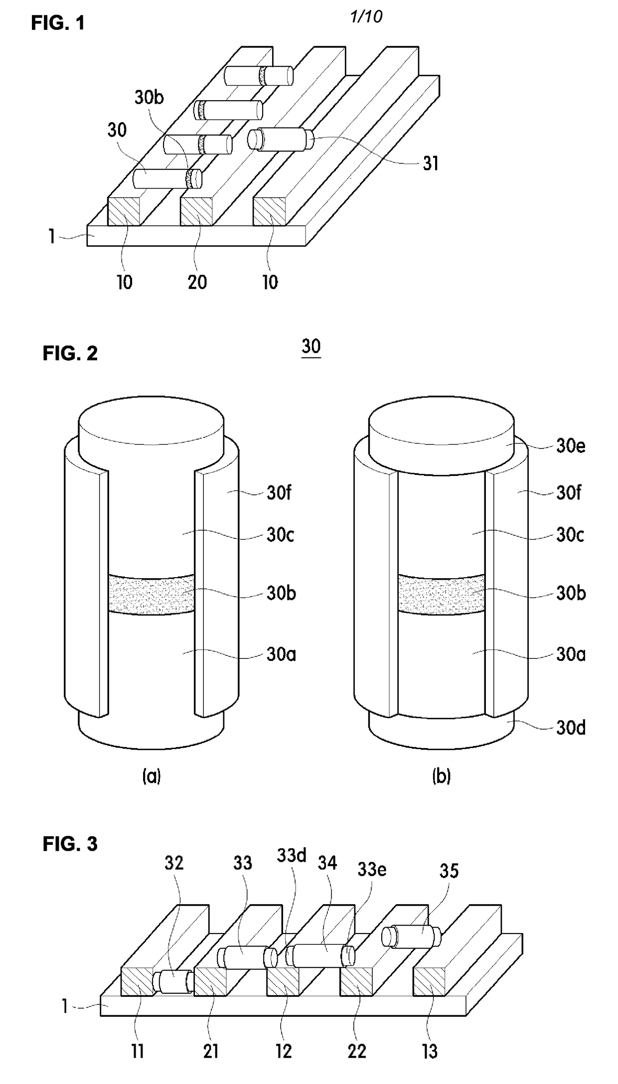
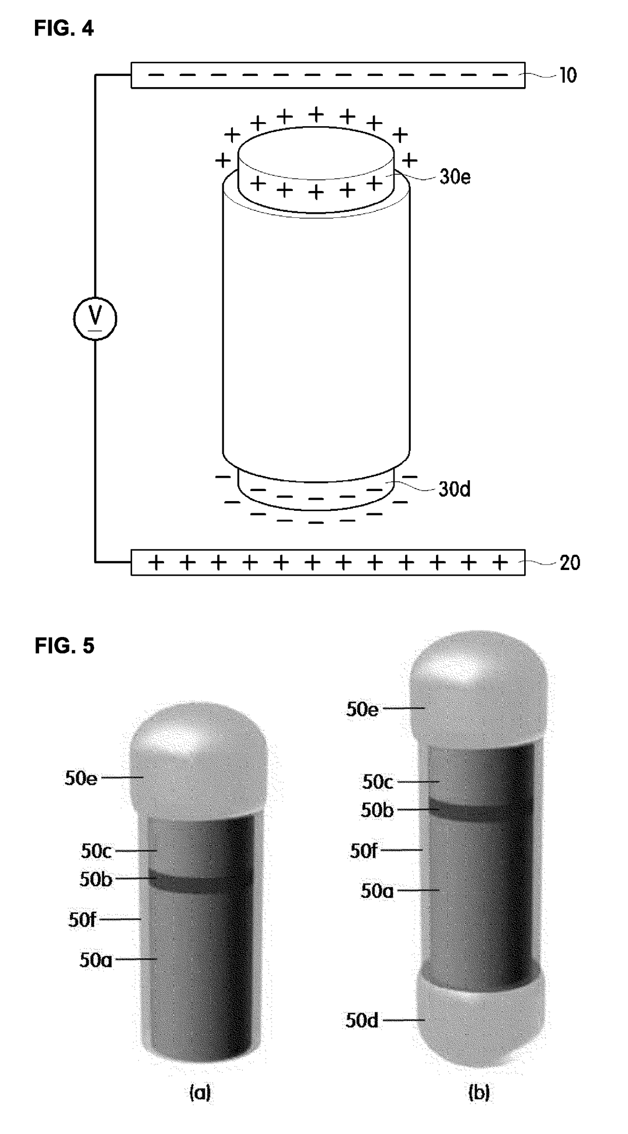
[0009]A first objective of the present invention is to provide a nano-scale light-emitting diode (LED) element for a horizontal array assembly that can be easily laid in a length direction and mounted on a desired electrode region, and a manufacturing method thereof. According to the present invention, it is possible to improve an alignment of LED elements mounted on a desired electrode region to significantly increase the number of LED elements that are included per unit area of an electrode line and significantly improve electrical connectivity between the electrode and the LED elements.

[0010]A second objective of the present invention is to provide a horizontal array assembly that can significantly increase the number of nano-scale LED elements that are mounted per unit area of an electrode line by utilizing the nano-scale LED element according to the present invention, and that can have a good e...


PUM


Abstract

The present invention relates to a nano-scale light-emitting diode (LED) element for a horizontal array assembly, a manufacturing method thereof, and a horizontal array assembly including the same, and more particularly, to a nano-scale LED element for a horizontal array assembly that can significantly increase the number of nano-scale LED elements connected to an electrode line, facilitate an arrangement of the elements, and implement a horizontal array assembly having a very good electric connection between an electrode and an element and a significant high quantity of light when a horizontal array assembly having the nano-scale LED elements laid in a length direction thereof and connected to the electrode line is manufactured, a manufacturing method thereof, and a horizontal array assembly including the same.

Description

TECHNICAL FIELD[0001]The present invention relates to a nano-scale light-emitting diode (LED) element for a horizontal array assembly, a method of manufacturing the same, and a horizontal array assembly including the same, and more particularly, to a nano-scale LED element for a horizontal array assembly that can significantly increase the number of nano-scale LED elements connected to an electrode line, facilitate an arrangement of elements thereof, and implement a horizontal array assembly having a very good electric connection between an electrode and an element and a significantly high quantity of light when a horizontal array assembly having the nano-scale LED elements laid in a length direction thereof and connected to the electrode line is manufactured, a manufacturing method thereof, and a horizontal array assembly including the same.BACKGROUND ART[0002]Light-emitting diodes (LEDs) have been actively developed since 1992 when Shuji Nakamura et al. of Nichia Corporation of Ja...

Claims


Application Information

Patent Timeline
IPC IPC(8): H01L33/00H01L33/06H01L33/44H01L33/38H01L33/24H01L33/32H01L33/08B82B3/00
CPCH01L33/0075H01L33/06H01L33/08H01L33/24B82B3/0052H01L33/44H01L33/38H01L2933/0025H01L2933/0016H01L33/32F21S4/00H01L25/0753H01L33/62H01L2933/0066H01L2224/95085H01L33/20H01L33/385H01L25/075H01L33/005H01L33/02H01L33/48
Inventor SUNG, YEON GOOG
Owner SAMSUNG DISPLAY CO LTD
Why Eureka
Try Eureka