Solid-state imaging device

a solid-state imaging and imaging device technology, applied in the direction of solid-state device signal generators, picture signal generators, television systems, etc., can solve the problems of poor light use efficiency, low sensitivity, poor resolution, etc., and achieve the effect of easy installation

Inactive Publication Date: 2007-03-22
FUJIFILM HLDG CORP +1
View PDF15 Cites 23 Cited by
  • Summary
  • Abstract
  • Description
  • Claims
  • Application Information

AI Technical Summary

Benefits of technology

[0037] According to the configuration, wirings can be easily laid.

Problems solved by technology

In a color imaging device in which color filters are arranged in a mosaic-like manner, in the case of filters of the primary colors, however, about two thirds of incident light is absorbed by the color filters, and there arises a problem in that the light use efficiency is poor and the sensitivity is low.
Since each light receiving portion can produce only a color signal of one color, there are other problems in that also the resolution is poor, and that a false color is particularly conspicuous.
The devices are hardly produced, and the production yield is low.
Consequently, there is a problem in that the production cost is high.
Consequently, there arises a problem in that spectral sensitivity characteristics for R, G, and B signals are not sufficiently separated from one another, and color reproducibility is poor.
There is another problem in that the S / N ratio of the image signal is impaired by the adding and subtracting processes.
However, a signal process circuit unit includes an analog amplifier and a CDS circuit, and occupies a large area.
Therefore, it is difficult to triplicate the integration degree while maintaining the chip size.
Consequently, the sensitivities and saturation outputs of R and B lights detected by the photodiodes are low, and the S / N ratios of the R and B signals are impaired.
When the S / N ratios of the R and B signals are reduced, however, the image quality (S / N ratio) of the whole is impaired.
As described above, in the case where a CMOS signal read circuit is used in a hybrid imaging device, it is difficult to realize an increased number of pixels and high sensitivity.

Method used


Image

  • Solid-state imaging device
  • Solid-state imaging device
  • Solid-state imaging device

Examples


first embodiment

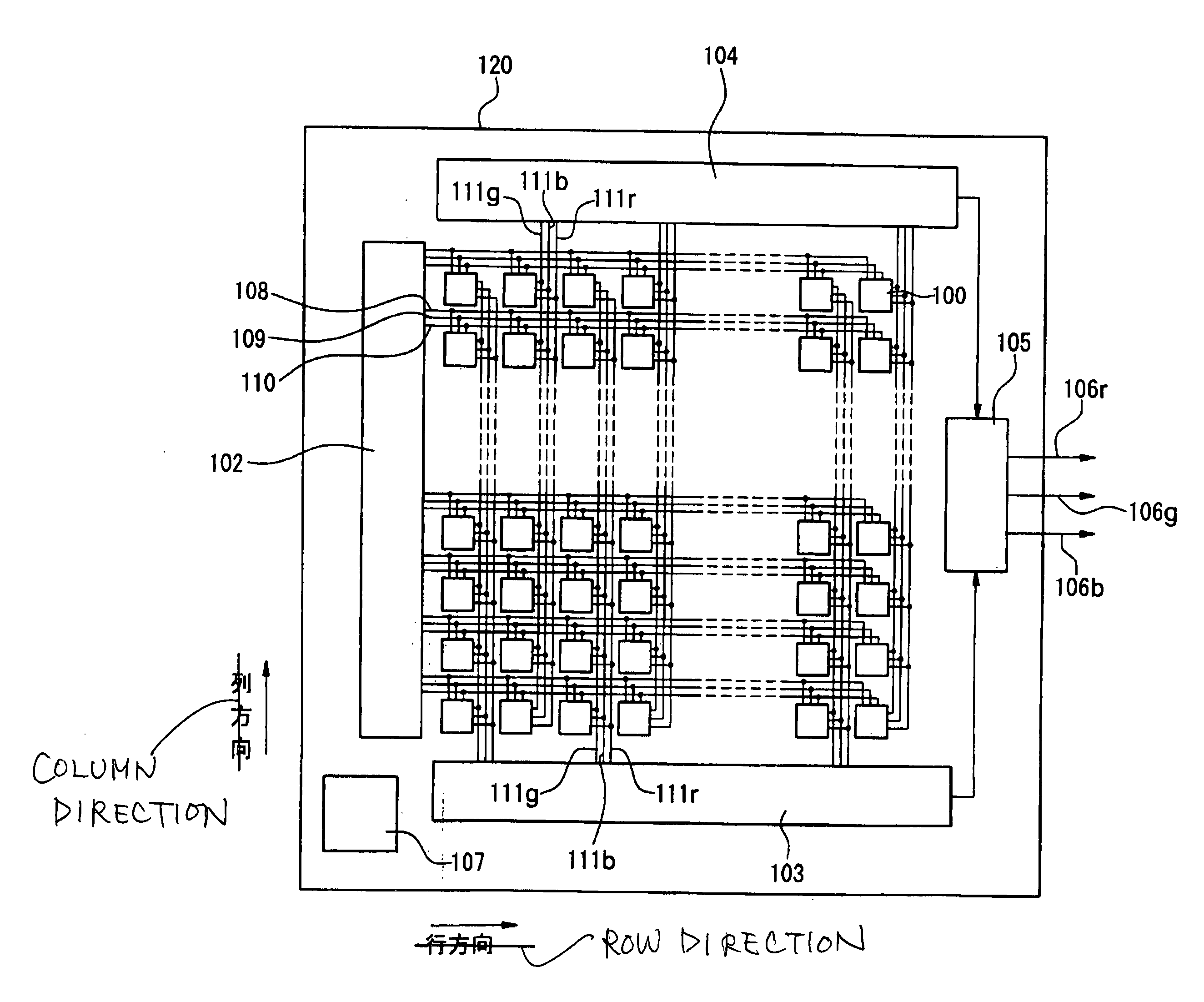
[0045]FIG. 1 is a surface diagram showing the configuration of a hybrid solid-state imaging device illustrating a first embodiment of the invention.

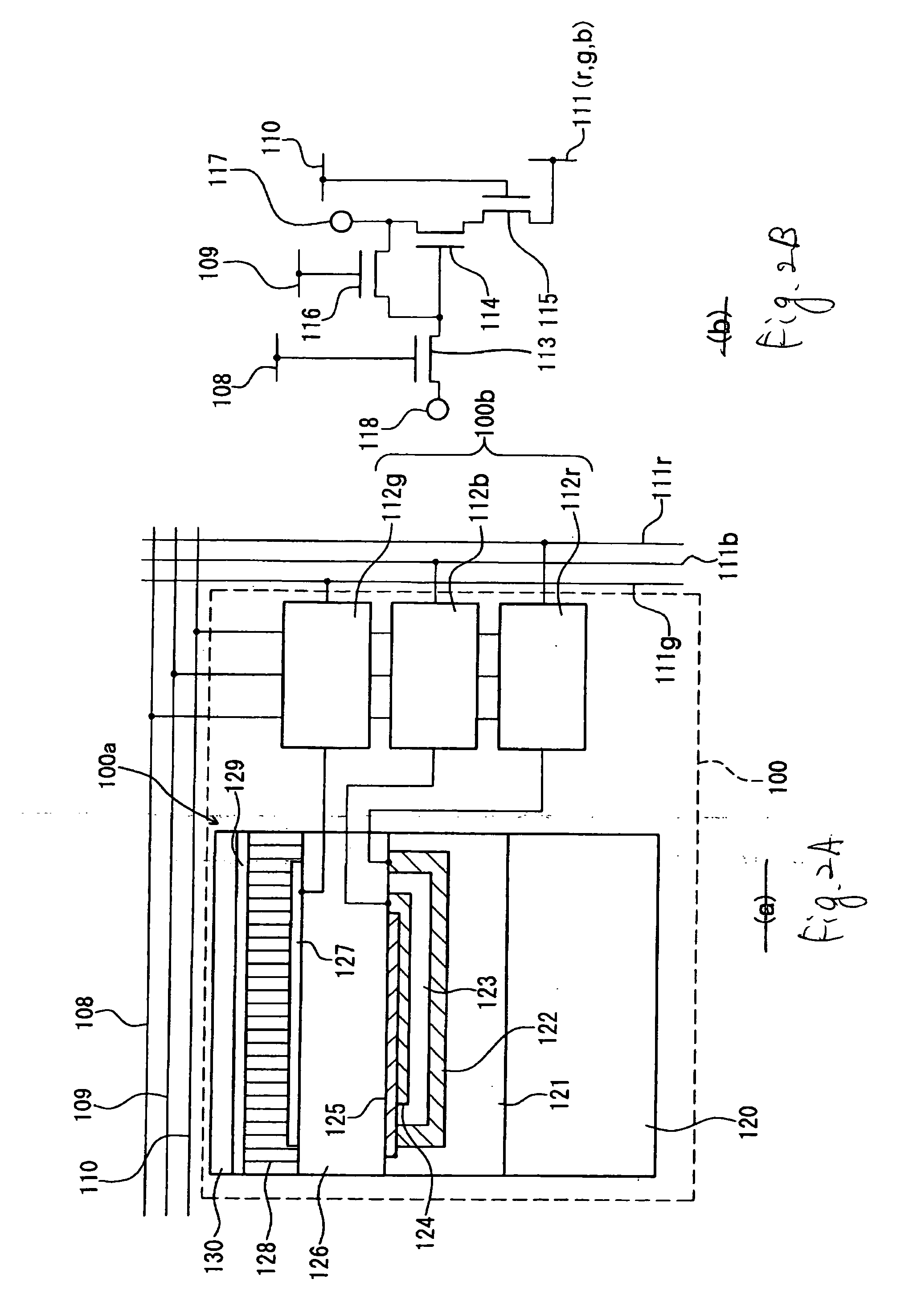
[0046] The solid-state imaging device shown in FIG. 1 comprises many pixels 100 which are arranged a square lattice pattern in a row direction in the figure and a column direction perpendicular to the row direction. The many pixels 100 are arranged so that a row configured by plural pixels 100 which are arranged in the row direction is set as a pixel row, and a large number of such pixel rows are arranged in the column direction, or that a column configured by plural pixels 100 which are arranged in the column direction is set as a pixel column, and a large number of such pixel columns are arranged in the row direction. Each of the pixels 100 includes: a light receiving portion which detects lights of R, G, and B to generate signal charges corresponding to the detected lights, and which accumulate the signal charges; and a signal read c...

second embodiment

[0076]FIG. 4 is a surface diagram showing the configuration of a hybrid solid-state imaging device illustrating a second embodiment of the invention.

[0077] The solid-state imaging device shown in FIG. 4 comprises many pixels 200 which are arranged in a square lattice pattern in a row direction in the figure and a column direction perpendicular to the row direction. The many pixels 200 are arranged so that pixel rows each configured by plural pixels 200 which are arranged in the row direction are arranged in the column direction, or that pixel columns each configured by plural pixels 200 which are arranged in the column direction are arranged in the row direction. Each of the pixels 200 includes: a light receiving portion which is configured in the same manner as that described in the first embodiment; a signal read circuit configured by MOS transistors for reading out color signals corresponding to the signal charges which are accumulated in the light receiving portion; and a MOS s...


PUM


Abstract

A solid-state imaging device comprising pixels arranged in a row direction and a column direction, wherein each of the pixels comprises: (i) a light receiving portion including photoelectric converting elements which are formed overlappingly in a depth direction of a semiconductor substrate, and which detect lights of different colors respectively, and a photoelectric converting film which is stacked above the plural photoelectric converting elements, and which detects a light of a color different from the colors detected by the photoelectric converting elements; and (ii) a signal read circuit which reads out signals corresponding to the lights detected by the photoelectric converting elements and the photoelectric converting film, wherein the solid-state imaging device comprises: a first signal processing section which applies a predetermined signal process on signals read out from first signal read circuits in a part of the pixels; and a second signal processing section which applies the predetermined signal process on signals read out from second signal read circuits in pixels other than the part of the pixels.

Description

BACKGROUND OF THE INVENTION [0001] 1. Field of the Invention [0002] The present invention relates to a solid-state imaging device having many pixels which are arranged in a row direction and a column direction perpendicular to the row direction. [0003] 2. Description of the Related Art [0004] In a single-type solid-state color imaging device which is typified by a CCD or CMOS image sensor, three or four kinds of color filters are arranged in a mosaic-like manner on the arrangement of light receiving portions which perform photoelectric conversion. According to the configuration, each of the light receiving portions outputs a color signal corresponding to the color filter, and the color signals are signal-processed to produce a color image. [0005] In a color imaging device in which color filters are arranged in a mosaic-like manner, in the case of filters of the primary colors, however, about two thirds of incident light is absorbed by the color filters, and there arises a problem in...

Claims


Application Information

Patent Timeline
Patent Type & Authority Applications(United States)
IPC IPC(8): H04N9/04
CPCH04N9/045H04N5/37457H04N25/778
Inventor SUZUKI, NOBUO
Owner FUJIFILM HLDG CORP
Why Eureka
Try Eureka