Antenna device, card information medium, electronic apparatus, and method for manufacturing antenna device

a technology of antenna device and card information medium, which is applied in the direction of loop antenna, radiating element structure, instruments, etc., can solve the problems of frequent short circuit between neighboring end surface conductors, short circuit between end surface conductors, etc., and achieve the effect of reducing or preventing the increase in conductor loss, preventing the short circuit between the end surface conductor and adjacent conductors

Active Publication Date: 2017-11-02
MURATA MFG CO LTD
View PDF2 Cites 0 Cited by
  • Summary
  • Abstract
  • Description
  • Claims
  • Application Information

AI Technical Summary

Benefits of technology

[0027]According to the above-described manufacturing method, the interval between the end-surface conductors adjacent to each other is increased, and the possibility of shorting between the end-surface conductors is lessened. The line width of the main portion in the linear conductor is able to be set at a predetermined width, and an increase in conductor loss is able to be reduced or prevented.
[0028]According to various preferred embodiments of the present invention, the antenna device, small card information medium, and electronic apparatus capable of preventing shorting between the end-surface conductors and of reducing or preventing an increase in conductor loss are obtainable.

Problems solved by technology

Typically, if a via conductor is exposed at an end surface of a multilayer body, a short circuit may be frequently caused by fine dust, faint printing, splatting of solder at the time of mounting, or the like.
In particular, if the end-surface via is formed by filling with electrode paste, the inserted electrode paste may extend to an adjacent end surface conductor, and this may lead to the risk of causing a short circuit between the neighboring end surface conductors.

Method used


Image

  • Antenna device, card information medium, electronic apparatus, and method for manufacturing antenna device
  • Antenna device, card information medium, electronic apparatus, and method for manufacturing antenna device
  • Antenna device, card information medium, electronic apparatus, and method for manufacturing antenna device

Examples


first preferred embodiment

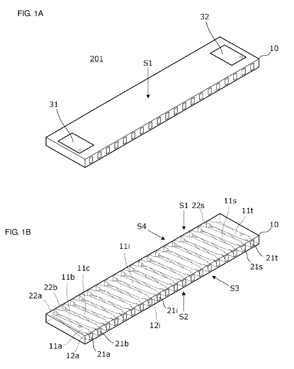
[0043]FIG. 1A is a perspective view of an antenna device 201 according to a first preferred embodiment of the present invention. FIG. 1B illustrates the structure inside the antenna device 201.

[0044]The antenna device 201 includes a multilayer body 10 having a rectangular or substantially rectangular parallelepiped shape. The multilayer body 10 includes a first principal surface S1, a second principal surface S2 opposed to the first principal surface S1, and end surfaces S3 and S4 connecting the first principal surface S1 and second principal surface S2. As illustrated in FIG. 1A, outer connection electrodes 31 and 32 are preferably disposed on the first principal surface S1 of the multilayer body 10. The antenna device 201 is surface-mounted on a circuit board by connecting the outer connection electrodes 31 and 32 to lands on the circuit board.

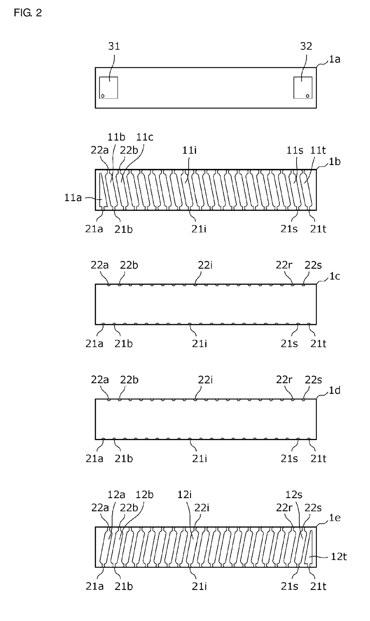
[0045]First linear conductors (including 11a-11c, 11i, 11s, and 11t) are disposed the first principal surface S1 side of the multilayer bod...

second preferred embodiment

[0089]In a second preferred embodiment, some example shapes of the first end portion and second end portion in the first linear conductor are illustrated. In the example illustrated in FIG. 8A, the line width of each of the first end portion 111 and second end portion 112 in the first linear conductor is smaller than the line width of the first main portion 110. In the example illustrated in FIG. 8B, each of the first end portion 111 and second end portion 112 has a frustum shape in which the line width tapers down from the first main portion 110. In the example illustrated in FIG. 8C, the portion 111R, which is near the first main portion 110, in the first end portion 111 has a line width larger than the line width of the portion 111E, which is remote from the first main portion 110, and smaller than the line width of the first main portion 110. Similarly, the portion 112R, which is near the first main portion 110, in the second end portion 112 has a line width larger than the line...

third preferred embodiment

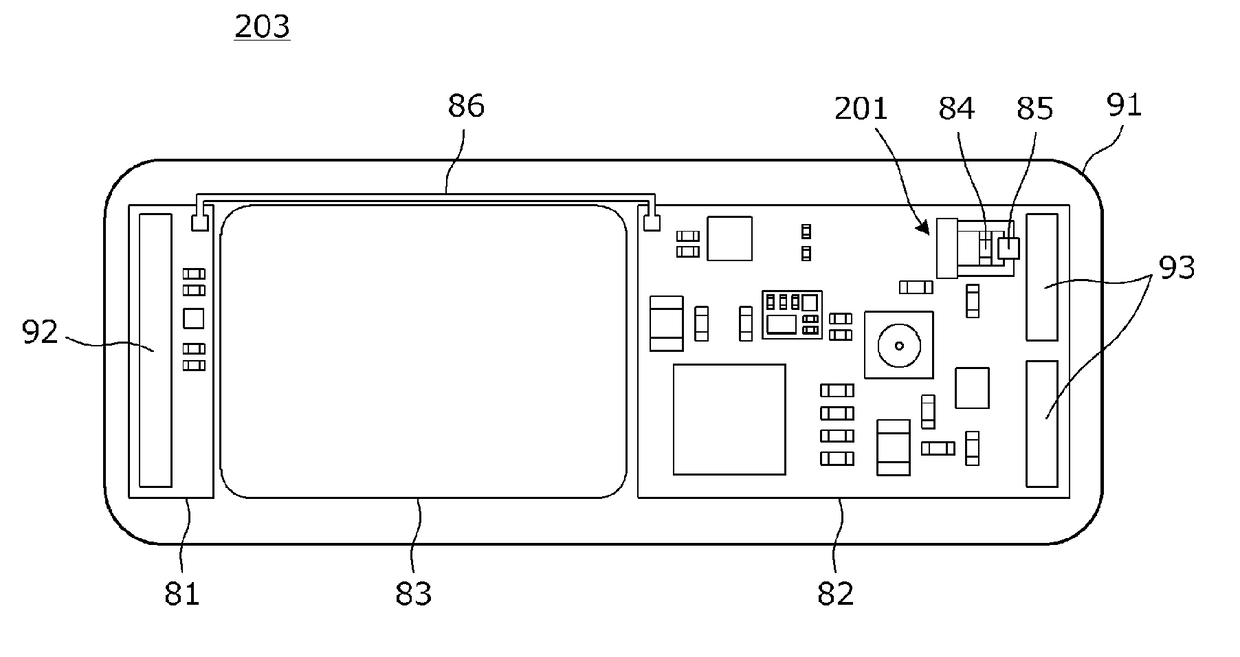
[0091]In a third preferred embodiment of the present invention, an example card information medium in the present invention is illustrated. FIG. 9A is a plan view of a card information medium according to the third preferred embodiment. FIG. 9B is an external perspective view of an electronic apparatus in which the card information medium is attachable.

[0092]The electronic apparatus preferably includes a casing 62 with a rectangular or substantially rectangular parallelepiped shape extending in the longitudinal direction and lateral direction and includes a card slot 63 that allows a card information medium 202 to be inserted therein and removed therefrom.

[0093]The card information medium 202 includes the antenna device 201 disposed therein. The card information medium 202 is a small card device attachable to and detachable from a terminal main body, such as a memory card, for example, a Secure Digital (SD) card (registered trademark), or a subscriber identity module (SIM) card. The...


PUM


Abstract

An antenna device includes a coil including first linear conductors on a first principal surface side of a multilayer body, second linear conductors on a second principal surface side, first end-surface conductors and second end-surface conductors disposed on end surfaces. Each of the first linear conductors includes a first main portion, a first end portion, and a second end portion. Each of the second linear conductors includes a second main portion, a third end portion, and a fourth end portion. The width of each of the first end-surface conductors is smaller than the width of the first main portion and the width of the second main portion. The width of each of the second end-surface conductors is smaller than the width of the first main portion and the width of the second main portion.

Description

CROSS REFERENCE TO RELATED APPLICATIONS[0001]This application claims the benefit of priority to Japanese Patent Application No. 2015-079408 filed on Apr. 8, 2015 and is a Continuation Application of PCT Application No. PCT / JP2016 / 061347 filed on Apr. 7, 2016. The entire contents of each application are hereby incorporated herein by reference.BACKGROUND OF THE INVENTION1. Field of the Invention[0002]The present invention relates to antenna devices, and in particular to an antenna device defining a chip coil antenna and a manufacturing method therefor. The present invention also relates to a card information medium and an electronic apparatus including an antenna device.2. Description of the Related Art[0003]A typical surface-mount antenna device including a coil antenna includes a helical coil formed of conductive patterns disposed on an insulating layer. Of the conductive patterns, a conductive pattern extending along the lamination direction is formed of a via hole (via conductor)....

Claims


Application Information

Patent Timeline
Patent Type & Authority Applications(United States)
IPC IPC(8): H01Q1/22G06K19/077H01Q1/38H01Q7/00
CPCH01Q1/22G06K19/07773H01Q1/38H01Q7/00H01F5/003G06K19/07779H01Q1/2275H01Q1/243H01Q1/273
Inventor TENNO, NOBUYUKI
Owner MURATA MFG CO LTD
Why Eureka
Try Eureka