Mounter and method for inspecting suction posture of electronic component using mounter

a technology of electronic components and mounters, which is applied in the direction of image analysis, image enhancement, instruments, etc., can solve the problems of electronic components that cannot be mounted on the board at the specified position, the electronic component is getting smaller, and the image processing accuracy is difficult to achieve good accuracy, so as to achieve accurate image processing, curtail the increase in image processing time, and improve the effect of image processing accuracy

Active Publication Date: 2017-11-02
FUJI MASCH MFG CO LTD
View PDF14 Cites 0 Cited by
  • Summary
  • Abstract
  • Description
  • Claims
  • Application Information

AI Technical Summary

Benefits of technology

[0010]The above head is provided internally with a component data acquiring section, an image processing section, and an image processing pattern selecting section. With this configuration too, it is possible to perform appropriately accurate image processing of small electronic components, while curtailing an increase in the image processing time.
[0011]Further, this specification discloses a new electronic component pickup orientation inspection method. This pickup orientation inspection method is a method for inspecting the pickup orientation of an electronic component picked up by a suction nozzle in a mounter that mounts an electronic component picked up by a suction nozzle at a specified location on a board. The pickup orientation inspection method includes a processing step, an imaging step, a selecting step, and an image processing step. In the acquiring step, the size of the electronic component picked up by the suction nozzle is acquired. In the imaging step, the pickup orientation of the electronic component picked up by the suction nozzle is imaged. In the selecting step, the image processing range and the image processing accuracy for the image captured in the imaging step are selected based on the size of the electronic component acquired in the acquiring step. In the image processing step, the image captured in the imaging step is image processed using the image processing range and the image processing accuracy selected in the selecting step. In the selecting step, it is possible to select one image processing range from multiple predetermined image processing ranges, it is possible to select one image processing accuracy from multiple predetermined processing accuracies, and, as the size of the electronic component acquired from the component data acquiring section becomes smaller, a smaller image processing range is selected from the multiple image processing ranges, and a more accurate image processing accuracy is selected from the multiple image processing accuracies. According to this inspection method, it is possible to perform appropriately accurate image processing of small electronic components, while curtailing an increase in the image processing time.

Problems solved by technology

Recently, electronic components are getting smaller.
Therefore, it is difficult to image process with good accuracy the pickup orientation of small components using conventional image processing accuracy.
If the pickup orientation of an electronic component cannot be image processed with good accuracy, the position correction amount, thickness, and so on of the electronic component cannot be calculated reliably, leading to a problem that the electronic component cannot be mounted on the board at the specified position.
As a result, the time required for image processing is short, but there is a problem in that image processing of the pickup orientation of the electronic component cannot be performed with good accuracy.
Also, generally, as the image processing accuracy improves, the image processing time per unit of surface area increases, but with the above configuration, when the image processing accuracy is high, the image processing range is made smaller, which curtails the time required for image processing the entire image processing range.

Method used


Image

  • Mounter and method for inspecting suction posture of electronic component using mounter
  • Mounter and method for inspecting suction posture of electronic component using mounter
  • Mounter and method for inspecting suction posture of electronic component using mounter

Examples


first embodiment

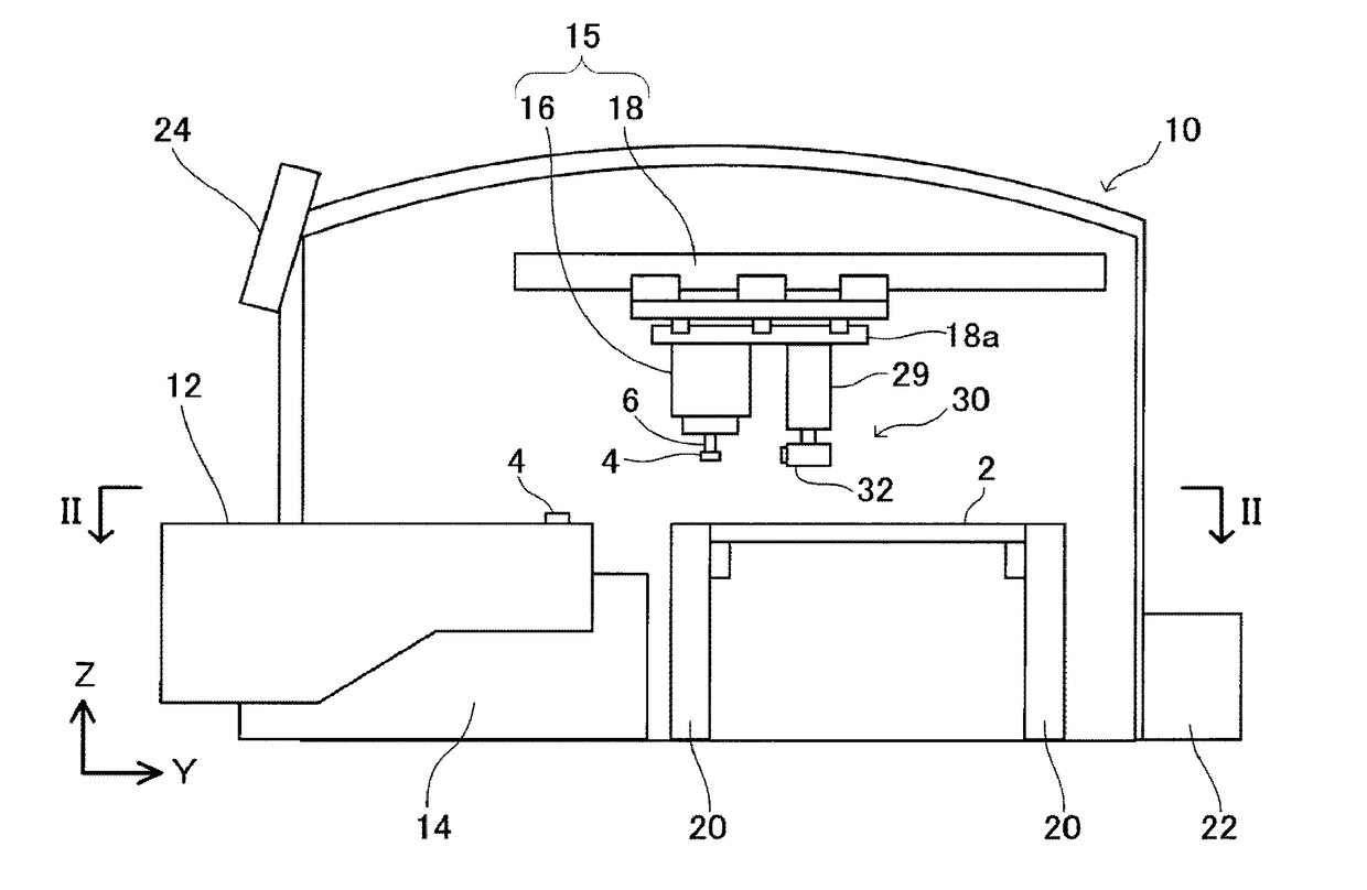
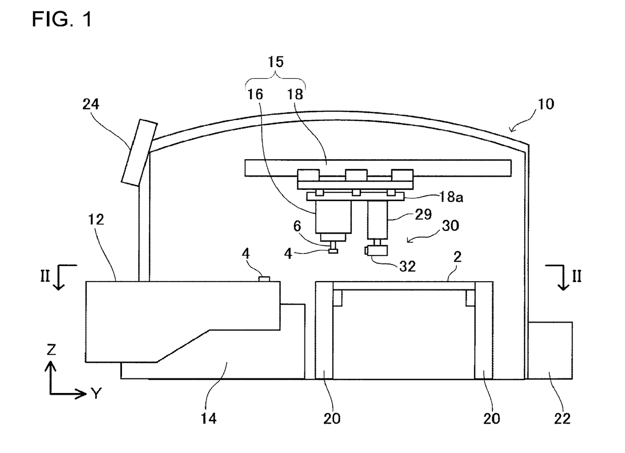
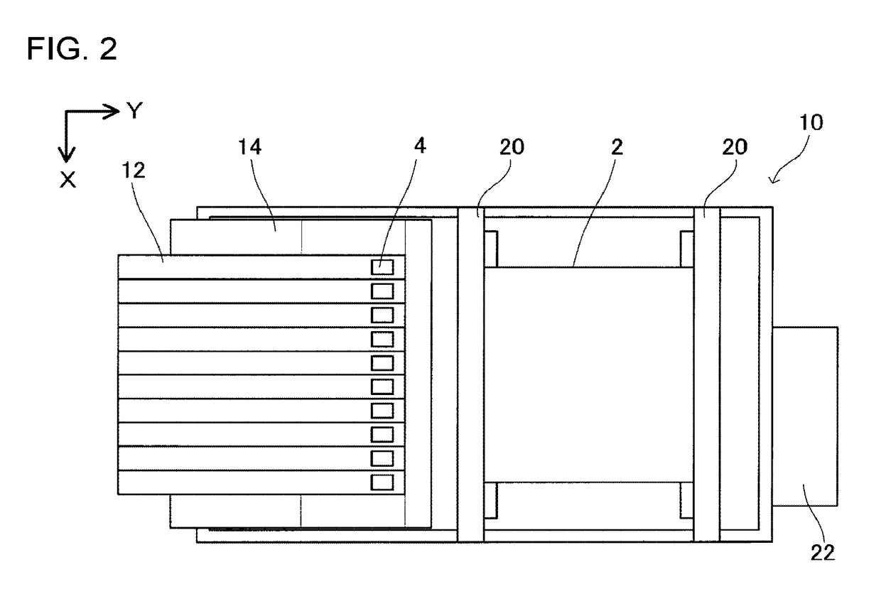
[0024]Mounter 10 of an embodiment is described with reference to the figures. Mounter 10 is a device that mounts electronic components 4 on circuit board 2. Mounter 10 is also known as an electronic component mounting device or a chip mounter. Usually, mounter 10 is set up with other board work machines such as a solder printer and board inspection machine to form a mounting line.

[0025]As shown in FIGS. 1 and 2, mounter 10 is provided with multiple component feeders 12, feeder holding section 14, head unit 15 configured from mounting head 16 and head moving device 18, imaging device 30, board conveyor 20, control device 22, and touch panel 24. Each component feeder 12 stores multiple electronic components 4. Component feeders 12 are detachably attached to feeder holding section 14, and supply electronic components 4 to mounting head 16. The specific configuration of component feeders 12 is not particularly limited. Each component feeder 12, for example, may be a tape type feeder tha...

embodiment 2

[0044]Next, head unit 115 of a second embodiment is described with reference to FIG. 8. Below, only elements that are different to the first embodiment are described, elements the same as the first embodiment are given the same reference signs and detailed descriptions thereof are omitted. Head unit 115 of the second embodiment is different from head unit 15 of the first embodiment with regard to the configuration using a computer that includes memory 40 and CPU 42. Imaging device 130 is an imaging device that images the pickup orientation of electronic component 4 picked up by nozzle 6, and is provided with the same configuration as image device 30 of the first embodiment. Imaging device 130 is fixed to moving base 18a (one configuration element of head unit 115) by fixing member 29, and moves together with moving base 18a. The same memorizing sections 44, 46, 48, and 49 as the first embodiment are provided in memory 40. Also, CPU 42 functions as sections 50, 52, 54, 56, and 58 the...


PUM


Abstract

A mounter is provided with a head unit with a suction nozzle capable of picking up an electronic component that transfers the electronic component to a specified position, an imaging device that images the pickup orientation of the electronic component, a component data acquiring device that acquires the size of the electronic component, an image processing section that image processes the captured image, and an image processing pattern selecting section. The image processing pattern selecting section, based on the size of the electronic component, is able to select one image processing range and one image processing accuracy from multiple predetermined image processing ranges and multiple predetermined printing accuracies, and, as the size of the electronic component acquired from the component data acquiring section becomes smaller, selects a smaller image processing range and a more accurate image processing accuracy from the multiple image processing ranges and multiple image processing accuracies.

Description

TECHNICAL FIELD[0001]Technology disclosed in the present specification relates to a mounter and method for inspecting the pickup orientation of an electronic component using the mounter.BACKGROUND ART[0002]Generally, mounters that mount electronic components on circuit boards are provided with a head unit, an imaging device, and an image processing section. The head unit includes suction nozzles capable of picking up electronic components, and transfers the electronic components to a specified position on a circuit board. The imaging device images the pickup orientation of the electronic component (hereinafter also referred to as a picked component) picked up by a suction nozzle. The image processing section image processes image data captured by the imaging device and calculates the position correction amount, thickness, and so on of the electronic component. The mounter mounts the electronic component based on the result calculated by the image processing section.[0003]Disclosed i...

Claims


Application Information

Patent Timeline
Patent Type & Authority Applications(United States)
IPC IPC(8): H05K13/08G06T7/00H05K13/04
CPCH05K13/08G06T2207/30141G06T7/0004H05K13/0408H05K13/0812H05K13/0813
Inventor FUKAYA, YOSHIYUKI
Owner FUJI MASCH MFG CO LTD
Why Eureka
Try Eureka