Light-Emitting Element, Display Device, Electronic Device, and Lighting Device

a technology of light-emitting elements and electronic devices, which is applied in the direction of semiconductor devices, solid-state devices, diodes, etc., can solve the problems of reducing the emission efficiency of light-emitting elements from iridium complexes, reducing the emission efficiency of light-emitting elements, and increasing the driving voltage of light-emitting elements, etc., to achieve low power consumption and high emission efficiency

Active Publication Date: 2017-11-23
SEMICON ENERGY LAB CO LTD
View PDF0 Cites 17 Cited by
  • Summary
  • Abstract
  • Description
  • Claims
  • Application Information

AI Technical Summary

Benefits of technology

[0030]One embodiment of the present invention can provide a light-emitting element with high emission efficiency. Another embodiment of the present invention can provide a light-emitting element with low power consumption. Another embodiment of the present invention can provide a novel light-emitting element. Another embodiment of the present invention can provide a novel light-emitting device. Another embodiment of the present invention can provide a novel display device.

Problems solved by technology

For this reason, in the iridium complex including a nitrogen-containing five-membered heterocyclic skeleton as a ligand, excitation of carriers by direct carrier recombination is difficult, which means that efficient light emission is difficult.
When the iridium complex and another compound form an exciplex, problems such as a decrease in the emission efficiency of light emitted from the iridium complex or an increase in the driving voltage of a light-emitting element are caused.

Method used


Image

  • Light-Emitting Element, Display Device, Electronic Device, and Lighting Device
  • Light-Emitting Element, Display Device, Electronic Device, and Lighting Device
  • Light-Emitting Element, Display Device, Electronic Device, and Lighting Device

Examples


embodiment 1

[0139]In this embodiment, a light-emitting element of one embodiment of the present invention is described below with reference to FIG. 1, FIGS. 2A to 2C, FIGS. 3A to 3C, and FIGS. 4A and 4B.

[0140]First, a structure of a light-emitting element of one embodiment of the present invention is described below with reference to FIG. 1.

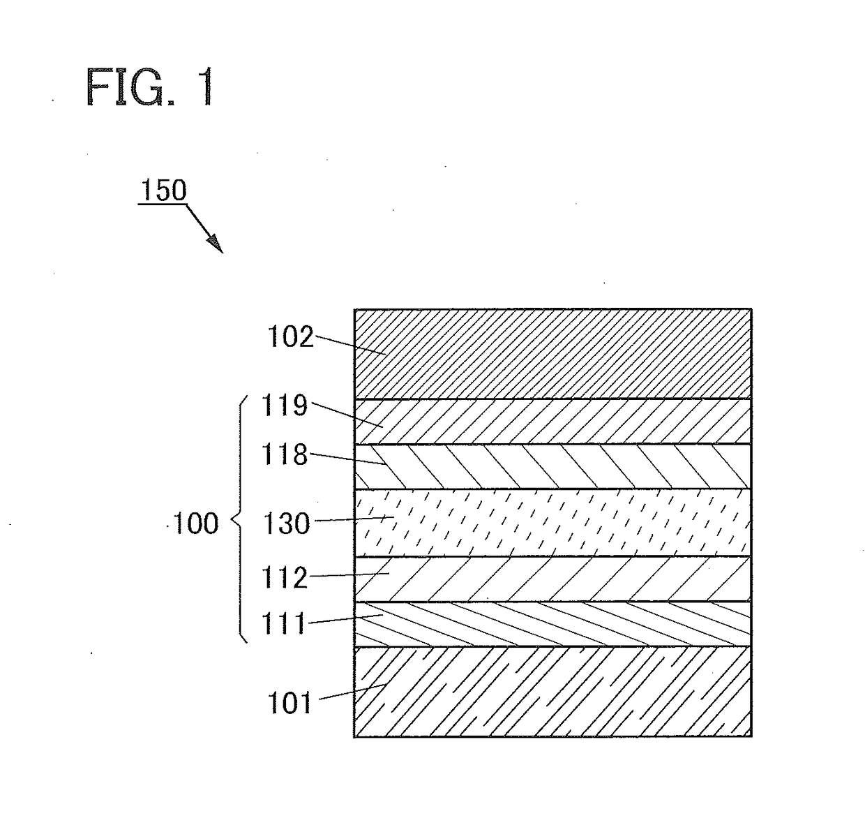
[0141]FIG. 1 is a schematic cross-sectional view of a light-emitting element 150 of one embodiment of the present invention.

[0142]The light-emitting element 150 includes a pair of electrodes (an electrode 101 and an electrode 102) and an EL layer 100 between the pair of electrodes. The EL layer 100 includes at least a light-emitting layer 130.

[0143]The EL layer 100 illustrated in FIG. 1 includes functional layers such as a hole-injection layer 111, a hole-transport layer 112, an electron-transport layer 118, and an electron-injection layer 119, in addition to the light-emitting layer 130.

[0144]Although description is given assuming that the electrode 101 and...

embodiment 2

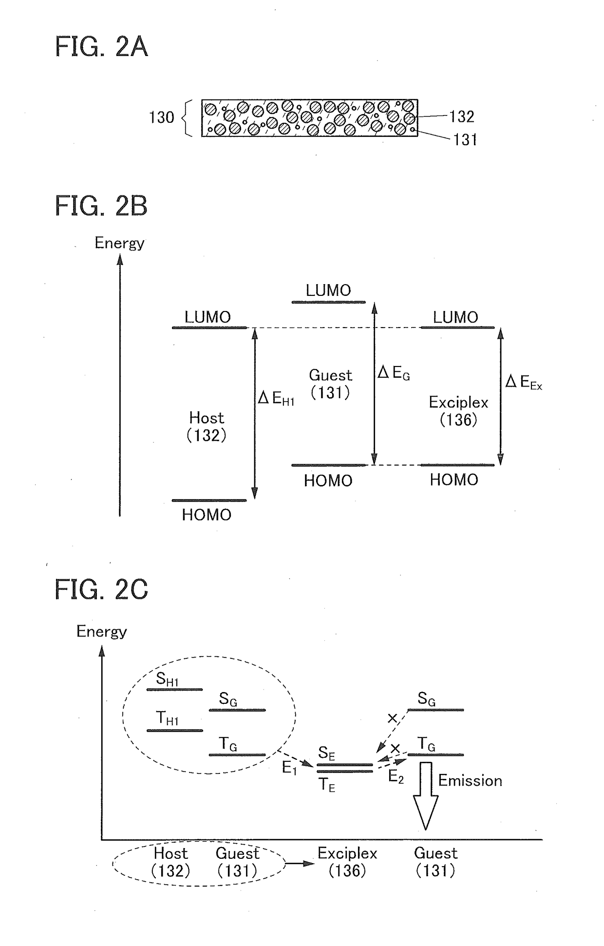
[0358]In this embodiment, a light-emitting element having a structure different from that described in Embodiment 1 and light emission mechanisms of the light-emitting element are described below with reference to FIG. 5. In FIG. 5, a portion having a function similar to that in FIG. 1 is represented by the same hatch pattern as in FIG. 1 and not especially denoted by a reference numeral in some cases. In addition, common reference numerals are used for portions having similar functions, and a detailed description of the portions is omitted in some cases.

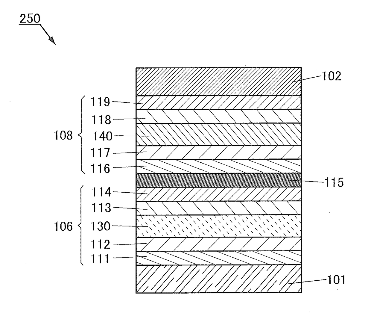
[0359]FIG. 5 is a schematic cross-sectional view of a light-emitting element 250.

[0360]The light-emitting element 250 illustrated in FIG. 5 includes a plurality of light-emitting units (a light-emitting unit 106 and a light-emitting unit 108 in FIG. 5) between a pair of electrodes (the electrode 101 and the electrode 102). One light-emitting unit has the same structure as the EL layer 100 illustrated in FIG. 1. That is, the light-em...

embodiment 3

[0375]In this embodiment, examples of light-emitting elements having structures different from those described in Embodiments 1 and 2 are described below with reference to FIG. 6 and FIGS. 7A and 7B.

[0376]FIG. 6 is a cross-sectional view of a light-emitting element of one embodiment of the present invention. In FIG. 6, a portion having a function similar to that in FIG. 1 is represented by the same hatch pattern as in FIG. 1 and not especially denoted by a reference numeral in some cases. In addition, common reference numerals are used for portions having similar functions, and a detailed description of the portions is omitted in some cases.

[0377]A light-emitting element 260 in FIG. 6 may have a bottom-emission structure in which light is extracted through a substrate 200 or may have a top-emission structure in which light emitted from the light-emitting element is extracted in the direction opposite to the substrate 200. However, one embodiment of the present invention is not limit...


PUM


Abstract

A light-emitting element having low driving voltage and high emission efficiency is provided. In the light-emitting element, a combination of a guest material and a host material forms an exciplex. The guest material is capable of converting triplet excitation energy into light emission. Light emission from the light-emitting layer includes light emission from the guest material and light emission from the exciplex. The percentage of the light emission from the exciplex to the light emission from the light-emitting layer is greater than 0 percent and less than or equal to 60 percent. The energy after subtracting the energy of light emission from the exciplex from the energy of light emission from the guest material is greater than 0 eV and less than or equal to 0.23 eV.

Description

TECHNICAL FIELD[0001]One embodiment of the present invention relates to a light-emitting element, or a display device, an electronic device, and a lighting device each including the light-emitting element.[0002]Note that one embodiment of the present invention is not limited to the above technical field. The technical field of one embodiment of the invention disclosed in this specification and the like relates to an object, a method, or a manufacturing method. In addition, one embodiment of the present invention relates to a process, a machine, manufacture, or a composition of matter. Specifically, examples of the technical field of one embodiment of the present invention disclosed in this specification include a semiconductor device, a display device, a liquid crystal display device, a light-emitting device, a lighting device, a power storage device, a memory device, a method for driving any of them, and a method for manufacturing any of them.BACKGROUND ART[0003]In recent years, re...

Claims


Application Information

Patent Timeline
Patent Type & Authority Applications(United States)
IPC IPC(8): H01L51/50H01L27/32H01L51/00
CPCH01L51/5016H01L51/5004H01L51/5056H01L51/5072H01L51/0084H01L27/322H01L51/0086H01L51/0087H01L51/0088H01L51/0085H10K59/30H10K59/35H10K59/38H10K85/342H10K50/11H10K2101/40H10K2101/10H10K50/852H10K50/19H10K2101/90H10K85/6572H10K50/15H10K50/16H10K85/341H10K85/344H10K85/346H10K85/348
Inventor MITSUMORI, SATOMIWATABE, TAKEYOSHISEO, SATOSHIKUBOTA, YUKO
Owner SEMICON ENERGY LAB CO LTD
Why Eureka
Try Eureka