Transparent conductive film and touch panel

Active Publication Date: 2017-12-21
FUJIFILM CORP
View PDF0 Cites 7 Cited by
  • Summary
  • Abstract
  • Description
  • Claims
  • Application Information

AI Technical Summary

Benefits of technology

[0023]According to the present invention, since the first thin metal wire of the first electrode has the first front surface that is directed to the viewing side and has a line width W1A, and the first back surface that is directed to the side opposite to the viewing side and has a line width W1B, and the second thin metal wire of the second electrode arranged on the side opposite to the viewing side from the first electrode has the second front surface that is directed to the viewing side and has the l

Problems solved by technology

Thus, there is a problem that the presence of the copper wirings 2 a

Method used


Image

  • Transparent conductive film and touch panel
  • Transparent conductive film and touch panel
  • Transparent conductive film and touch panel

Examples


embodiment 1

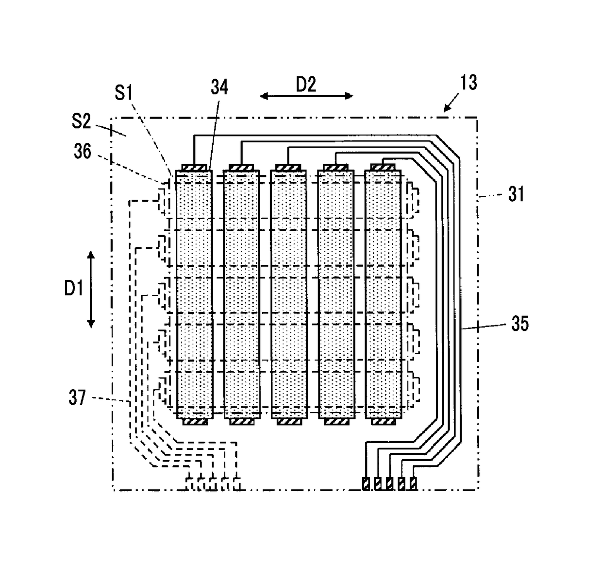
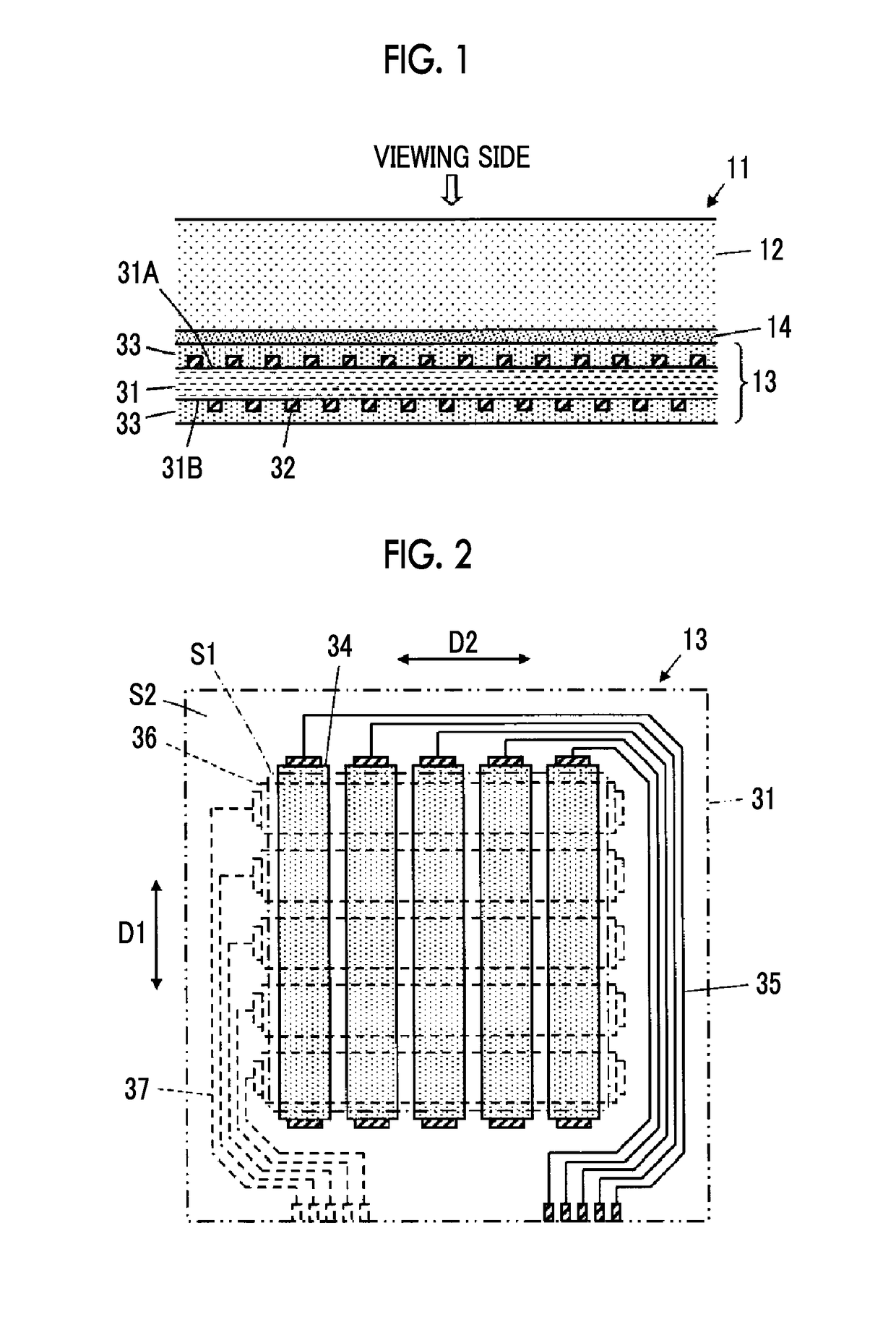
[0032]FIG. 1 shows a configuration of a touch panel 11 using a transparent conductive film 13 according to Embodiment 1 of the present invention. The touch panel 11 has a transparent insulating cover panel 12 having a flat plate shape, and the transparent conductive film 13 is bonded to a surface of the cover panel 12 on a side opposite to a viewing side with a transparent adhesive 14. In the transparent conductive film 13, a conductive member 32 is formed on both surfaces of the transparent insulating substrate 31, that is, on a front surface 31A and on a rear surface 31B, respectively. In addition, as shown in FIG. 1, for the purpose of flattening or protecting the conductive member 32, a transparent protective layer 33 may be formed on both surfaces of the transparent insulating substrate 31 so as to cover the conductive member 32.

[0033]As the material for the cover panel 12, tempered glass, polycarbonate (PC), a polymethyl methacrylate resin (PMMA), or the like can be used and a...

embodiment 2

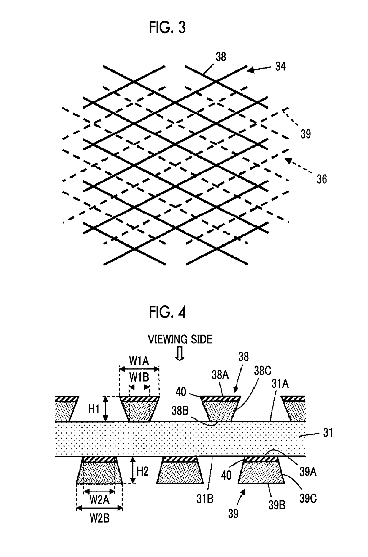
[0065]The transparent conductive film 13 used for the touch panel 11 of Embodiment 1 above has the blackened layers 40 respectively formed on the first front surface 38A of the first thin metal wire 38 on the viewing side and on the second front surface 39A of the second thin metal wire 39 on the viewing side, but the present invention is not limited thereto. For example, as shown in FIG. 5, the first thin metal wire 38 and the second thin metal wire 39 may not have the blackened layers 40.

[0066]Even in this case, as long as all of the line widths W1A and W1B of the first thin metal wire 38 and the line widths W2A and W2B of the second thin metal wire 39 are set to be in a range of 0.5 to 10 μm and satisfy the above relationship represented by Formula (1), the first thin metal wire 38 and the second thin metal wire 39 are hardly visually recognized and thus excellent visibility can be ensured.

[0067]In addition, the line width W1A of the first thin metal wire 38 and the line width W2...

embodiment 3

[0068]In Embodiments 1 and 2, as shown in FIG. 3, the first thin metal wire 38 of the first electrode 34 arranged on the front surface 31A of the transparent insulating substrate 31 and the second thin metal wire 39 of the second electrode 36 arranged on the rear surface 31B of the transparent insulating substrate 31 respectively have a mesh pattern, but the present invention is not limited thereto. For example, the transparent conductive film can also be configured such that as shown in FIG. 6, the first electrodes 34 are formed of a plurality of first thin metal wires 48 that are respectively bent and parallel with one another, the second electrodes 36 are formed of a plurality of second thin metal wires 49 that are respectively bent and parallel with one another, and in the case in which the transparent conductive film is viewed from the viewing side, the plurality of first thin metal wires 48 and the plurality of second thin metal wires 49 overlap each other to form a large numb...


PUM

PropertyMeasurementUnit
Thicknessaaaaaaaaaa
Thicknessaaaaaaaaaa
Electrical conductoraaaaaaaaaa

Abstract

A transparent conductive film having a transmissive region includes a first electrode formed of a first thin metal wire arranged in the transmissive region; and a second electrode formed of a second thin metal wire arranged on a side opposite to a viewing side from the first electrode so as to intersect the first thin metal wire in the transmissive region, in which the first thin metal wire has a first front surface that is directed to the viewing side and has a line width W1A, and a first back surface that is directed to the side opposite to the viewing side and has a line width W1B, the second thin metal wire has a second front surface that is directed to the viewing side and has a line width W2A, and a second back surface that is directed to the side opposite to the viewing side and has a line width W2B, and the line widths W1A, W1B, W2A, and W2B are in a range of 0.5 to 10 μm, and the line widths satisfy a relationship of W1B<W2A≦W1A<W2B.

Description

CROSS-REFERENCE TO RELATED APPLICATIONS[0001]This application is a Continuation of PCT International Application No. PCT / JP2015 / 79031, filed on Oct. 14, 2015, which claims priority under 35 U.S.C. §119(a) to Japanese Patent Application No. 2015-58283, filed on Mar. 20, 2015. Each of the above application(s) is hereby expressly incorporated by reference, in its entirety, into the present application.BACKGROUND OF THE INVENTION1. Field of the Invention[0002]The present invention relates to a transparent conductive film and particularly to a transparent conductive film used for a touch panel or the like.[0003]In addition, the present invention relates to a touch panel using a transparent conductive film.2. Description of the Related Art[0004]In recent years, in various electronic devices such as a portable information device, a touch panel that can be used in combination with a display device such as a liquid crystal display device and performs an input operation to an electronic devic...

Claims


Application Information

Patent Timeline
IPC IPC(8): G02F1/1333G06F3/041G02F1/1343
CPCG02F1/13338G02F1/1343G06F3/041G06F2203/04103B32B2307/412B32B2457/208B32B2307/202B32B7/12B32B7/14B32B17/06B32B27/08B32B27/308B32B27/325B32B27/36B32B27/365B32B2250/02B32B2250/24B32B2255/10B32B2255/20B32B2255/205B32B2307/416B32B2307/732G06F2203/04107G06F3/0445
Inventor NAKAYAMA, MASAYASUTOU, MAKOTO
Owner FUJIFILM CORP
Why Eureka
Try Eureka