Wired circuit board and producing method thereof

a wired circuit board and circuit board technology, applied in the field of wired circuit boards, can solve the problems that the formation of insufficient wiring patterns cannot be prevented, and achieve the effects of excellent connection reliability, excellent connection reliability, and excellent connection reliability

Active Publication Date: 2018-01-11
NITTO DENKO CORP
View PDF6 Cites 0 Cited by
  • Summary
  • Abstract
  • Description
  • Claims
  • Application Information

AI Technical Summary

Benefits of technology

[0021]However, with the method, in the step (4), the light shield portion of the photomask is disposed to deviate from the center, and therefore, even if the light reflected at the metal thin film corresponding to the arc is focused on the photoresist corresponding to the center of the virtual circle along the arc, light focusing on the portion, where the conductive pattern is to be provided in the photoresist, can be avoided (suppressed).
[0056]The wired circuit board of the present invention has excellent connection reliability.

Problems solved by technology

Then, there are disadvantages in that inadequate formation of the wiring pattern cannot be prevented.

Method used


Image

  • Wired circuit board and producing method thereof
  • Wired circuit board and producing method thereof
  • Wired circuit board and producing method thereof

Examples


first embodiment

[0128]The wired circuit board of the present invention has a single layer or a plurality of layers of the conductive pattern, and its layer structure is not particularly limited. The wired circuit board includes a suspension board with circuits including a metal supporting board, and a flexible wired circuit board (FPC) including no metal supporting board.

[0129]In the following, a first embodiment of the wired circuit board and its production method of the present invention are described sequentially.

[0130]1. Wired Circuit Board

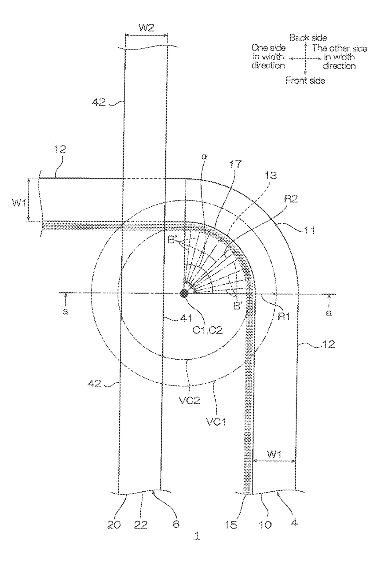
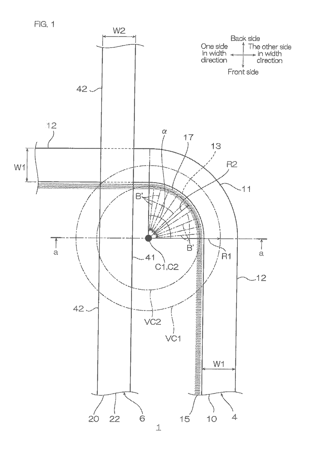
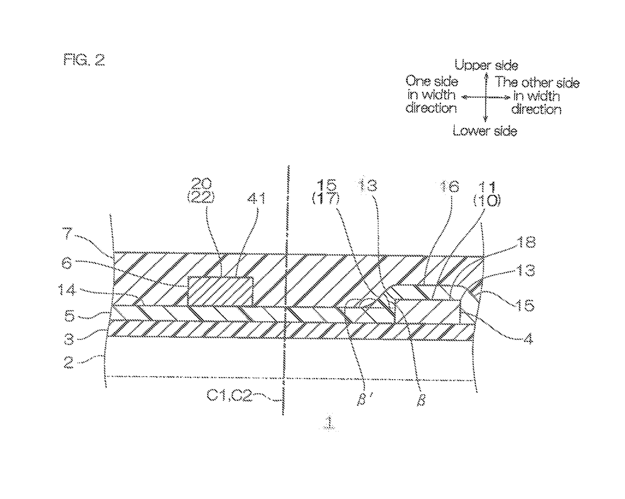
[0131]As shown in FIG. 1 and FIG. 2, a wired circuit board 1 includes the insulating base layer 3, the first conductive pattern 4 provided on the insulating base layer 3 as an example of the conductive pattern, the intermediate insulating layer 5 provided on the insulating base layer 3 as an example of the insulating layer and covering the first conductive pattern 4, the second conductive pattern 6 disposed on the intermediate insulating layer 5 as an example...

second embodiment

[0233]In the second embodiment, for the members and steps that are the same as the first embodiment, the same reference numerals are given and detailed descriptions thereof are omitted.

[0234]In the first embodiment, the negative type photoresist 25 is used, and the additive method is used to form the second conductive pattern 6.

[0235]However, in the second embodiment, the positive type photoresist 25 is used, and the subtractive method is used to form the second conductive pattern 6.

[0236]3-1. Method for Producing a Wired Circuit Board

[0237]The production method of the wired circuit board 1 in the second embodiment includes a step (i) (ref: FIG. 3A), in which the insulating base layer 3 of the first embodiment is prepared, a step (ii) (ref: FIG. 3B), in which the first conductive pattern 4 is provided, and a step (1) (ref: FIG. 3C), in which the intermediate insulating layer 5 is provided.

[0238]The production method of the wired circuit board 1 of the second embodiment further inclu...

third embodiment

[0268]In the third embodiment, for the members and steps that are the same as the first and second embodiments, the same reference numerals are given and detailed descriptions thereof are omitted.

[0269]As shown in FIG. 1 and FIG. 2, in the wired circuit board 1 of the first embodiment, the second wire 20 crosses the first linear portion 12.

[0270]However, as shown in FIG. 13, in the third embodiment, the second wire 20 has an L-shaped portion that does not cross the first linear portion 12. That is, the second wire 20 is disposed at the inner side of the first wire 10 in spaced-apart relation when viewed from the top.

[0271]The second wire 20 integrally includes a curve portion 19 and two second linear portions 22 that are connected to both ends thereof.

[0272]The curve portion 19 is an inner side portion 41 as an example of the inner circle portion positioned at an inner side of the virtual circle VC2 along the first arc portion 11. The curve portion 19 is bent in one side in the widt...


PUM


Abstract

A method of producing a wired circuit board including an insulating layer and a conductive pattern, including: (1), an insulating layer having an inclination face, (2), a metal thin film provided at least on the inclination face, (3), a photoresist provided on the surface of the metal thin film, (4), a light shield portion of a photomask disposed so that a first portion, where the conductive pattern is to be provided in the photoresist, is shielded from light, and the photoresist is exposed to light through the photomask, (5), the first portion of the photoresist is removed to expose the metal thin film corresponding to the first portion, and (6), the conductive pattern is provided on the surface of the metal thin film exposed from the photoresist.

Description

CROSS-REFERENCE TO RELATED APPLICATION[0001]This patent application is a divisional patent application of U.S. patent application Ser. No. 15 / 463,538, filed Mar. 20, 2017, which claims priority from Japanese Patent Application No. 2016-069039 filed on Mar. 30, 2016, the contents of all of which are hereby incorporated by reference into this application.BACKGROUND OF THE INVENTIONField of the Invention[0002]The present invention relates to a wired circuit board and a production method thereof, in particular, to a method for producing a wired circuit board, and a wired circuit board produced by the method.Description of Related Art[0003]It has been known that a wired circuit board is produced by providing an insulating layer and a wiring pattern thereon.[0004]For example, Japanese Unexamined Patent Publication No. 2014-127216 has proposed a method for producing a suspension board with circuit: the method includes a step of forming a first portion having a first thickness and a second ...

Claims


Application Information

Patent Timeline
Patent Type & Authority Applications(United States)
IPC IPC(8): H05K1/02H05K3/46H05K1/05H05K3/06
CPCH05K2203/0562H05K3/4644H05K1/0274H05K1/05H05K3/064H05K1/0284G11B5/486H05K1/0278H05K1/056H05K3/108H05K2203/052H05K3/0008H05K3/06H05K3/4679H05K2201/09227H05K2201/09272H05K2203/0557H05K2203/056
Inventor SUGIMOTO, YUUFUJIMURA, YOSHITOTANABE, HIROYUKI
Owner NITTO DENKO CORP
Why Eureka
Try Eureka