This helps you quickly interpret patents by identifying the three key elements:
Problems solved by technology
Method used
Benefits of technology
Benefits of technology
The present disclosure aims to provide an electroluminescent display device with better image quality and lower power consumption. It also enhances the lifetime of the display device.
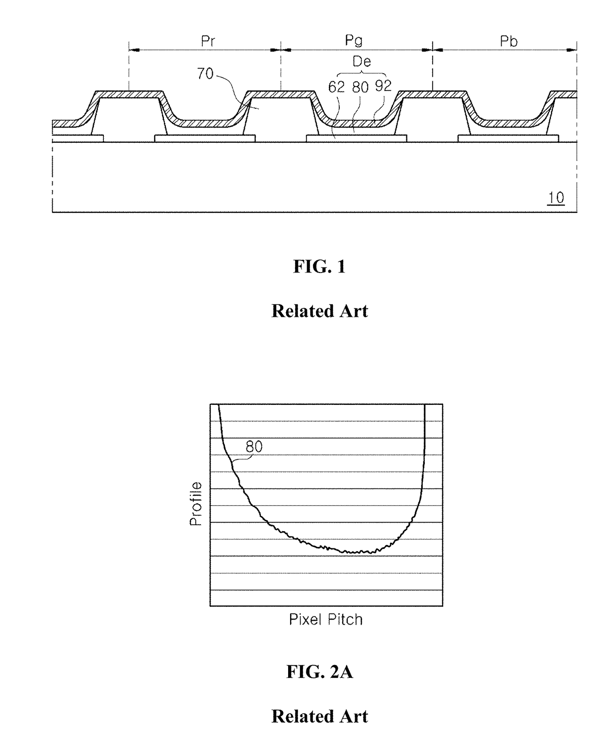
In addition, when the light emitting layer 80 has the asymmetric U-like shape of FIG. 2A, the driving voltage of the light emitting diode increases, and the power consumption also increases.
However, additional materials and apparatus are needed, and the manufacturing costs are increased.
Method used
Image
Click on the blue label to locate the original text in one second.
Reading with bidirectional positioning of images and text.
Examples
first embodiment
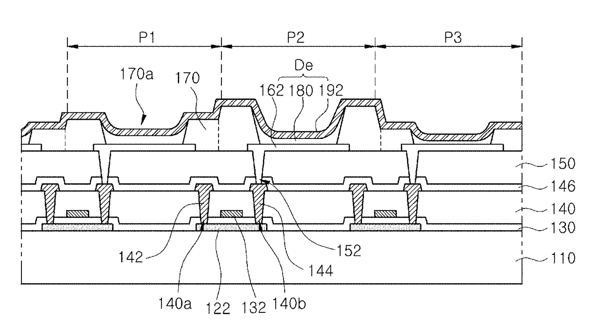
[0043]FIG. 4 is a cross-sectional view of an electroluminescent display device according to a first embodiment of the present disclosure and shows a plurality of pixel regions.
[0044]In FIG. 4, a plurality of pixel regions, for example, first, second and third pixel regions P1, P2 and P3 are defined on an insulating substrate 110. A semiconductor layer 122 is formed on the substrate 110 corresponding to each pixel region P1, P2 and P3. The substrate 110 can be a glass substrate or a plastic substrate.
[0045]The semiconductor layer 122 can be formed of an oxidesemiconductor material. In addition, the electroluminescent display device including the semiconductor layer 122 formed of an oxide semiconductor material can include a light-blocking pattern and a buffer layer formed under the semiconductor layer 122. The light-blocking pattern blocks light from the outside or light emitted from a light emitting diode to prevent the semiconductor layer 122 from being degraded by the light. Alte...
second embodiment
[0095]FIG. 7 is a schematic cross-sectional view of an electroluminescent display device according to the second embodiment of the present disclosure.
[0096]In FIG. 7, first, second and third pixel regions P1, P2 and P3 are defined on a substrate 210, and a passivation layer 250 is formed on the substrate 210.
[0097]Here, the first, second and third pixel regions P1, P2 and P3 have substantially the same size. For example, the first, second and third pixel regions P1, P2 and P3 can correspond to red, green and blue pixel regions, respectively.
[0098]The passivation layer 250 has a groove 254 corresponding to the second pixel region P2. At this time, the passivation layer 250 can correspond to the second passivation layer 150 of FIG. 4.
[0099]Meanwhile, one or more thin film transistors are formed between the substrate 210 and the passivation layer 250 to correspond to each pixel region P1, P2 and P3. The thin film transistors can have, but are not limited to, the same structure as those...
PUM
Abstract
An electroluminescent display device includes a substrate on which first and second pixel regions are defined, a passivation layer over the substrate, a first electrode in each of the first and second pixel regions on the passivation layer, a bank layer exposing the first electrode, a light emitting layer on the first electrode exposed by the bank layer, and a second electrode on the light emitting layer, wherein the bank layer includes first and second openings exposing the first electrodes corresponding to the first and second pixel regions, respectively, and a depth of the second opening is larger than a depth of the first opening.
Description
CROSS-REFERENCE TO RELATED APPLICATION[0001]The present application claims priority from and the benefit under 35 U.S.C §119(a) of Korean Patent Application Nos. 10-2016-0097257 filed on Jul. 29, 2016 and 10-2016-0182643 filed on Dec. 29, 2016, all of which are hereby incorporated by reference in their entirety.BACKGROUNDField of the Disclosure[0002]The present disclosure relates to an electroluminescent display device, and more particularly, to an electroluminescent display device, which increases color purity and light extraction efficiency and has a high image quality.Discussion of the Related Art[0003]Recently, flat panel displays have been widely developed and applied to various fields because of their thin profile, light weight, and low power consumption.[0004]Among the flat panel displays, electroluminescent display devices emit light due to the radiative recombination of an exciton after forming the exciton from an electron and a hole by injecting charges into a light emitti...
Claims
Application Information
Patent Timeline
Application Date:The date an application was filed.
Publication Date:The date a patent or application was officially published.
First Publication Date:The earliest publication date of a patent with the same application number.
Issue Date:Publication date of the patent grant document.
PCT Entry Date:The Entry date of PCT National Phase.
Estimated Expiry Date:The statutory expiry date of a patent right according to the Patent Law, and it is the longest term of protection that the patent right can achieve without the termination of the patent right due to other reasons(Term extension factor has been taken into account ).
Invalid Date:Actual expiry date is based on effective date or publication date of legal transaction data of invalid patent.

