Cleaning method, method of manufacturing semiconductor device and substrate processing apparatus

Active Publication Date: 2018-02-15
NTT MOBILE COMM NETWORK INC
View PDF4 Cites 2 Cited by
  • Summary
  • Abstract
  • Description
  • Claims
  • Application Information

AI Technical Summary

Benefits of technology

The invention provides a method to prevent damage to exhaust pipes caused by cleaning gas. This is achieved by gradually decreasing the flow rate of the cleaning gas while the temperature of the connection portion reaches a certain level. This technique helps to protect the exhaust pipes from damage and improve the overall production efficiency.

Problems solved by technology

When the film formation process is performed, some undesirable deposits may be adhered to the inside of the processing chamber.

Method used


Image

  • Cleaning method, method of manufacturing semiconductor device and substrate processing apparatus
  • Cleaning method, method of manufacturing semiconductor device and substrate processing apparatus
  • Cleaning method, method of manufacturing semiconductor device and substrate processing apparatus

Examples


modified example

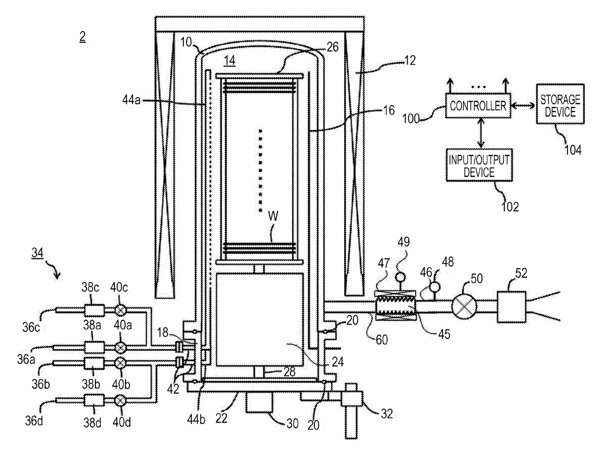
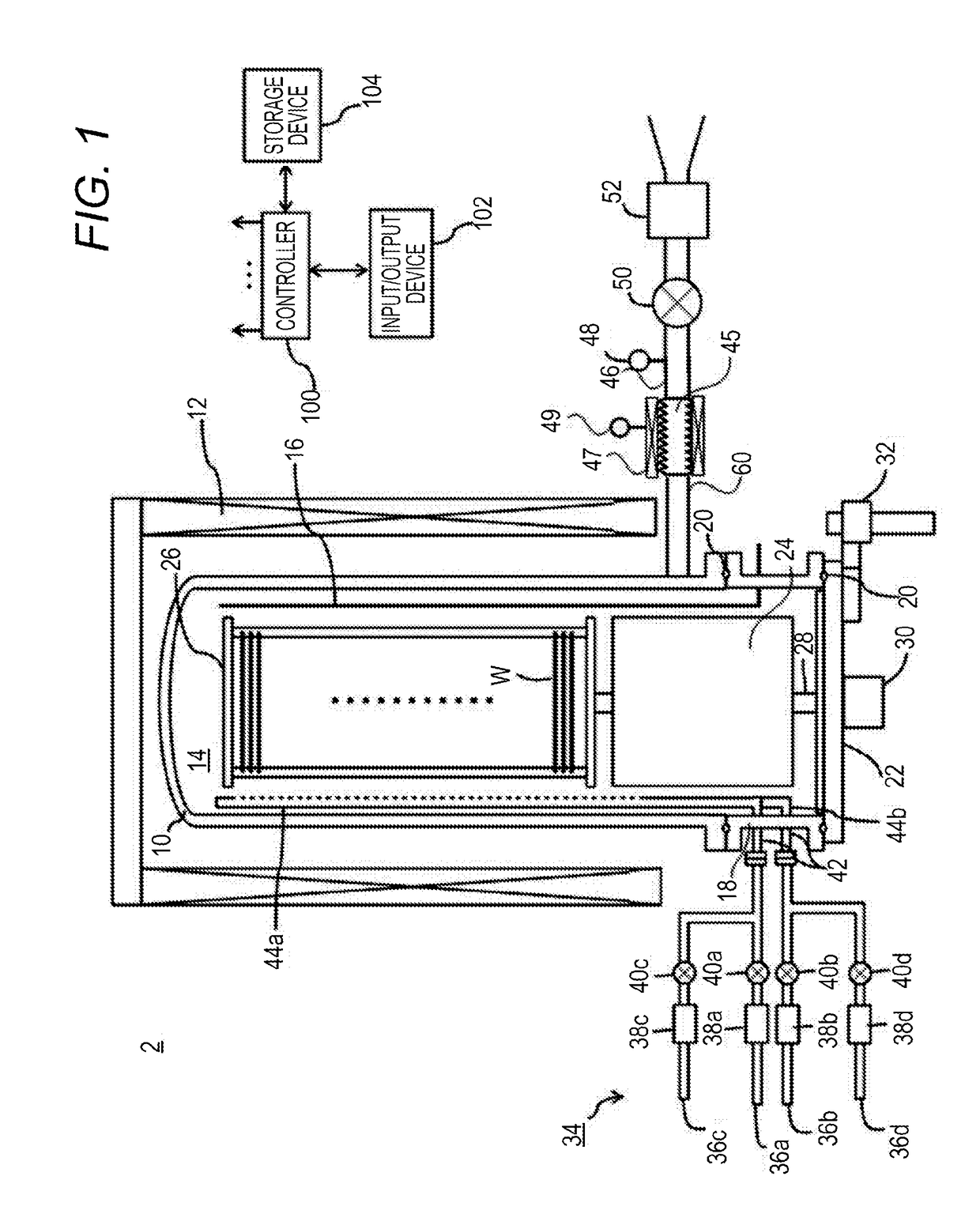
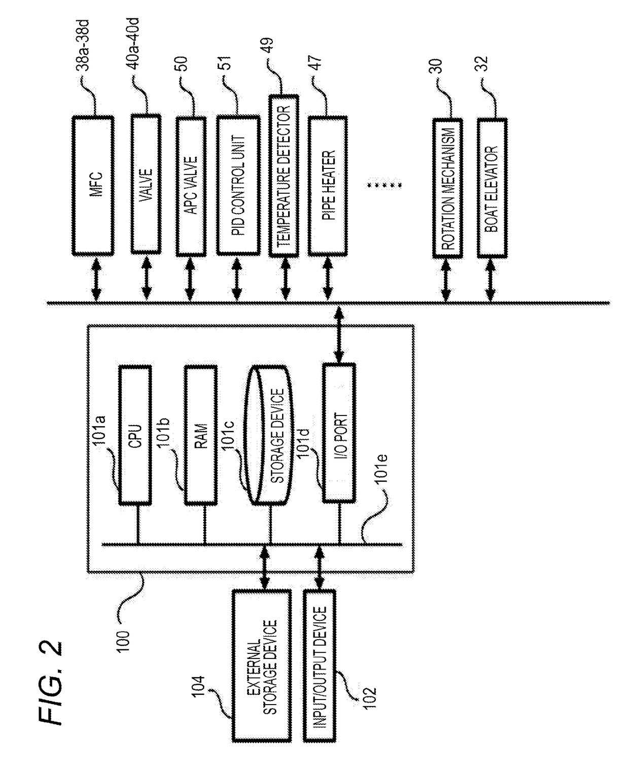
[0075]In the above-described embodiment, the flow rate of the cleaning gas is controlled so that the temperature of the exhaust connection portion 45 does not exceed the tolerance temperature, but the flow rate of the cleaning gas may be controlled so that the reaction amount between the deposits and the cleaning gas in the exhaust connection portion 45 do not exceed the threshold value.

[0076]It is preferable that the above-mentioned threshold value is a threshold value of the removal amount of deposits in the exhaust connection portion 45 (or the amount of reaction between the deposits and the cleaning gas) when the exhaust connection portion 45 exceeds the tolerance temperature by the reaction heat in the exhaust connection portion 45. The temperature gradient of the exhaust connection portion 45 depends on (1) the internal temperature of the processing chamber and (2) the reaction heat in the exhaust connection portion 45. Therefore, the temperature gradient A of the exhaust conn...


PUM

PropertyMeasurementUnit
Temperatureaaaaaaaaaa
Pressureaaaaaaaaaa
Flow rateaaaaaaaaaa

Abstract

A cleaning method includes: removing deposits adhered to an inside of a processing vessel by forming a film on a substrate in the processing vessel, and thereafter, supplying a cleaning gas into the processing vessel, wherein the removing the deposits includes: a first step of supplying the cleaning gas into the processing vessel at a first flow rate when a temperature of a connection portion connecting an exhaust pipe that exhausts the interior of the processing vessel and the processing vessel is lower than a first temperature; and a second step of supplying the cleaning gas to the processing vessel while gradually decreasing the flow rate of the cleaning gas from the first flow rate to a second flow rate lower than the first flow rate when the temperature of the connection portion reaches a first temperature.

Description

BACKGROUNDTechnical Field[0001]The present invention relates to a cleaning method, a method of manufacturing a semiconductor device, and a substrate processing apparatus.Related Art[0002]As one process of a plurality processes of manufacturing a semiconductor device, sometimes, a film formation process may be performed in which a source gas or a reaction gas is supplied to a substrate in a processing chamber to form a film on the substrate. When the film formation process is performed, some undesirable deposits may be adhered to the inside of the processing chamber. For this reason, after the film formation process, sometimes, a cleaning process may be carried out in which a cleaning gas is supplied into the processing chamber to remove the deposits accumulate on the inside of the processing chamber. In the cleaning process, sometimes, damage such as corrosion is given to an exhaust pipe by the cleaning gas (refer to, for example, JP 2014-170786 A).SUMMARY[0003]The invention is made...

Claims


Application Information

Patent Timeline
IPC IPC(8): C23C16/56B08B5/00B08B9/08
CPCC23C16/56B08B5/00B08B9/08H01L21/02041H01L21/02057H01L21/67023C23C16/345C23C16/4405C23C16/45546C23C16/45578C23C16/52
Inventor YAMAGUCHI, TAKATOMOSASAKI, TAKAFUMIKURIBAYASHI, KOEI
Owner NTT MOBILE COMM NETWORK INC
Why Eureka
Try Eureka