Organic Transistor, Method for Producing the Same and OLED Display Device

Active Publication Date: 2018-02-15
BOE TECH GRP CO LTD +1
View PDF2 Cites 0 Cited by
  • Summary
  • Abstract
  • Description
  • Claims
  • Application Information

AI Technical Summary

Benefits of technology

[0006]One of objectives of the present application is to provide an organic transistor, a method for producing the same and an OLED

Problems solved by technology

Since carriers of the organic materials have low mobility, they a

Method used


Image

  • Organic Transistor, Method for Producing the Same and OLED Display Device
  • Organic Transistor, Method for Producing the Same and OLED Display Device
  • Organic Transistor, Method for Producing the Same and OLED Display Device

Examples


Embodiment Construction

[0046]Below, technical solutions of embodiments of the present application will be described clearly and completely in conjunction with drawings for the embodiments. Apparently, the described embodiments are only a part of all embodiments of the present application, rather than all of the embodiments. From the embodiments of the present application, all other embodiments which can be obtained by the person skilled in the art without any inventive efforts belong to the scope of the present application.

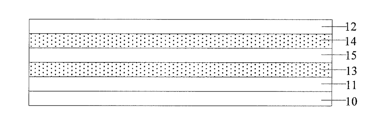
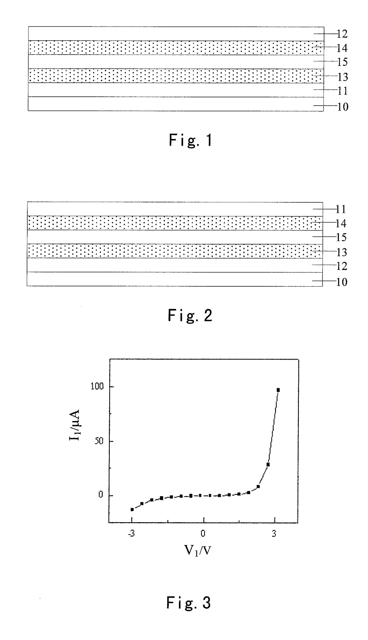
[0047]An embodiment of the present application provides an organic transistor, as shown in FIGS. 1 and 2. It includes a collector 11 and an emitter 12 stacked above a substrate 10; and a first organic semiconductor layer 13, a second organic semiconductor layer 14 and a base 15 between the first and second organic semiconductor layers 13 and 14. The first organic semiconductor layer 13, the second organic semiconductor layer 14 and the base 15 are stacked between the collector 11 and th...


PUM


Abstract

Embodiments of the present disclosure provide an organic transistor, a method for producing the same and an OLED display device. The organic transistor includes: a collector and an emitter stacked above a substrate; a first organic semiconductor layer, a second organic semiconductor layer and a base between the first and second organic semiconductor layers, stacked and provided between the collector and the emitter; wherein the base forms a Schottky contact with the first organic semiconductor layer and forms a Schottky contact with the second organic semiconductor layer.

Description

CROSS-REFERENCE TO RELATED APPLICATION[0001]This application is a Section 371 National Stage of International Application No. PCT / CN2016 / 086388, filed on 20 Jun. 2016, which has not yet published, and claims priority to Chinese Patent Application No. 201610166468.7, entitled with “an Organic Transistor, Method for Producing the Same and OLED Display Device” and filed with SIPO on Mar. 22, 2016, which is incorporated herein by reference in their entirety.BACKGROUND OF THE DISCLOSUREField of the Disclosure[0002]The present disclosure relates to technical field of display, and in particular, to an organic transistor, a method for producing the same and an OLED display device.Description of the Related Art[0003]Because Organic Light Emitting Diodes (abbreviated as OLEDs) display devices have advantages such as vivid color, ultra-thin thickness, energy conservation, a wide visual angle or the like, they are deemed to be a new generation display technique.[0004]For Active-Matrix Organic L...

Claims


Application Information

Patent Timeline
IPC IPC(8): H01L27/32H01L51/56H01L51/52H01L51/50
CPCH01L27/326H01L27/3274H01L51/508H01L51/56H01L51/5253H01L51/5064H01L2227/323H10K59/121H10K10/00H10K10/82H10K59/125H10K10/23H10K50/156H10K50/166H10K50/844H10K59/00H10K71/00H10K59/1201
Inventor ZHANG, HAO
Owner BOE TECH GRP CO LTD
Why Eureka
Try Eureka