Techniques for reducing electrical interconnection losses between a transmitter optical subassembly (TOSA) and associated driver circuitry and an optical transceiver system using the same

a technology of optical sub-assembly and optical transceiver, which is applied in the field of optical transceiver housing, can solve the problems of scaling down while maintaining nominal transceiver performan

Active Publication Date: 2018-03-01
APPLIED OPTOELECTRONICS
View PDF2 Cites 16 Cited by
  • Summary
  • Abstract
  • Description
  • Claims
  • Application Information

AI Technical Summary

Problems solved by technology

The desire to provide higher speeds in smaller optical transceiver modules for a lower cost has presented challenges, for example, with respect to maintaining optical efficiency (power), thermal management, insertion loss,

Method used


Image

  • Techniques for reducing electrical interconnection losses between a transmitter optical subassembly (TOSA) and associated driver circuitry and an optical transceiver system using the same
  • Techniques for reducing electrical interconnection losses between a transmitter optical subassembly (TOSA) and associated driver circuitry and an optical transceiver system using the same
  • Techniques for reducing electrical interconnection losses between a transmitter optical subassembly (TOSA) and associated driver circuitry and an optical transceiver system using the same

Examples


Embodiment Construction

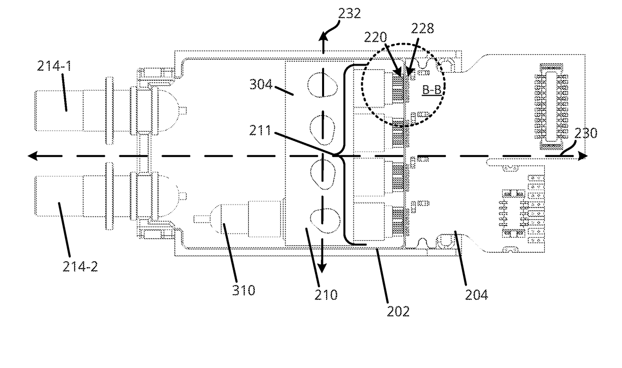
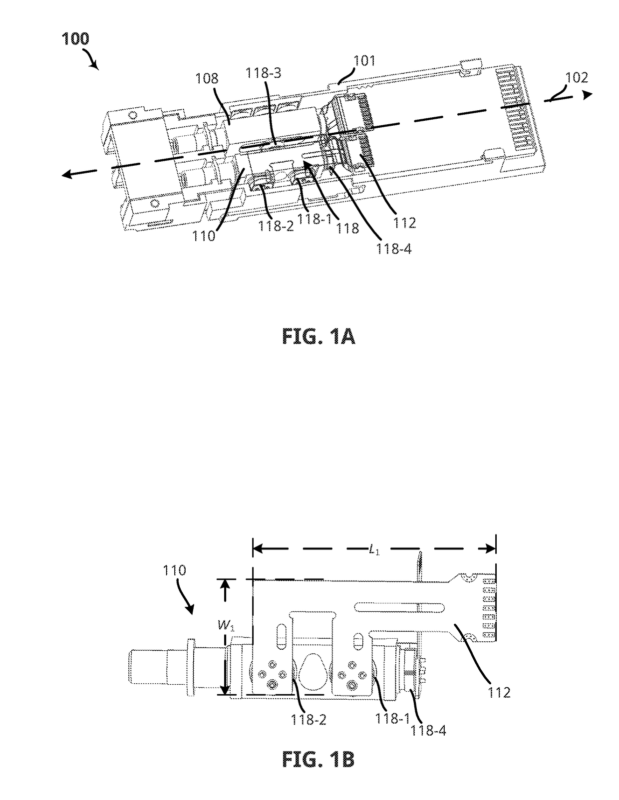
[0016]Increased demand for high-speed optical transceivers, largely due to the adoption of network standards such as IEEE 802.3bm-2015 and others that prescribe 100 Gigabit Ethernet (100 GbE) and beyond, raises non-trivial challenges in the design of optical subassembly modules. For example, the INF-8074i titled “Specification for SFP (Small Form factor Pluggable) Transceiver” adopted by the SFF Committee on May 12, 2001 established specific standard physical dimensions for optical transceivers that included a height of 8 millimeters (mm), a width of 13.4 mm and a depth (or length) of 56.5 mm. Other standards, such as INF-8077i titled “10 Gigabit Small Form Factor Pluggable Module” adopted by the Small Form Factor Committee in Aug. 31, 2005 also have standardized similarly constrained housing dimensions. In any event, these housing constraints further complicate increasing optical transceiver performance due to heat management issues, manufacturing complexity and losses introduced a...


PUM


Abstract

Techniques are disclosed for providing relatively short distances between multi-channel transmitter optical subassemblies (TOSAs) and associated transmit connecting circuit in order to reduce losses due to signal propagation delays, also sometimes referred to as signal flight time delays. In an embodiment, a TOSA includes a plurality of laser assemblies disposed along a same sidewall of the TOSA along a longitudinal axis. The TOSA may be disposed within an optical transceiver housing in a transverse orientation, whereby a longitudinal center line of the multi-channel TOSA is substantially perpendicular to the longitudinal axis of the optical transceiver housing. The TOSA may be positioned adjacent an end of the optical transceiver housing having a transmit connecting circuit. Thus each of the plurality of laser assemblies may be positioned at a relatively short distance, e.g., 120 microns or less, away from the transmit connecting circuit.

Description

CROSS-REFERENCE TO RELATED APPLICATIONS[0001]The present application is related to co-pending U.S. patent application Ser. No. ______, (Attorney Docket No. PAT260-08_AOI120) titled “An Optical Component Assembly With a Vertical Mounting Structure for Multi-Angle Light Path Alignment and an Optical Subassembly Using the Same” filed on Aug. 31, 2016, the entire disclosure of which is incorporated herein by reference.TECHNICAL FIELD[0002]The present disclosure generally relates to optical transceiver modules, and more particularly, to an optical transceiver housing having a multi-channel transmitter optical subassembly (TOSA) with laser assemblies disposed along a same sidewall of the multi-channel TOSA to allow for placement of the multi-channel TOSA within the optical transceiver that minimizes or otherwise reduces the distance, and by extension electrical signal propagation or flight time, between each laser assembly and a transmit connecting circuit configured to drive the same.BAC...

Claims


Application Information

Patent Timeline
IPC IPC(8): H04B10/572G02B6/42H04B10/50H04J14/02H01S5/12
CPCH04B10/572G02B6/4249G02B6/428H01S5/12H04J14/02G02B6/29365G02B6/2938H04B10/503H01S5/4087H04B10/40H04J14/0227
Inventor HO, I-LUNGWANG, CHONGLIANG, YONGXUAN
Owner APPLIED OPTOELECTRONICS
Why Eureka
Try Eureka