Substrate processing method and substrate processing apparatus

a substrate processing and substrate technology, applied in the direction of edge grinding machines, manufacturing tools, lapping machines, etc., can solve the problems of reducing yield, unnecessary film(s) or surface roughness on the peripheral portion of the substrate, and conventional polishing apparatus, etc., to achieve high-precision processing

Active Publication Date: 2018-03-15
EBARA CORP
View PDF14 Cites 18 Cited by
  • Summary
  • Abstract
  • Description
  • Claims
  • Application Information

AI Technical Summary

Benefits of technology

[0006]According to embodiments of the present invention to be described below, there are provided a substrate processing method and a substrate processing apparatus which are capable of forming a stepped recess highly accurately in a peripheral portion of a substrate.
[0022]In an embodiment, the substrate processing apparatus further comprises a position detector configured to detect a position of an outermost contour of the substrate on the stage surface, wherein the relatively-moving mechanism configured to move one of the substrate stage and the laser head in a direction as to eliminate a change in a distance between the outermost contour and the laser head while the substrate stage is rotating.
[0027]According to the embodiments described above, a laser beam creates a crack in an edge portion of a substrate. Since the crack serves as a boundary of a stepped recess to be formed in a peripheral portion of the substrate, the stepped recess can be formed highly accurately in the peripheral portion of the substrate.

Problems solved by technology

Therefore, an unnecessary film(s) or surface roughness is formed on a peripheral portion of the substrate.
With such a background, an unnecessary film, remaining on a peripheral portion of a substrate, may peel off during various processes and may adhere to a device formed on the substrate, resulting in reduced yield.
However, there are several problems in the conventional polishing apparatus.

Method used


Image

  • Substrate processing method and substrate processing apparatus
  • Substrate processing method and substrate processing apparatus
  • Substrate processing method and substrate processing apparatus

Examples


Embodiment Construction

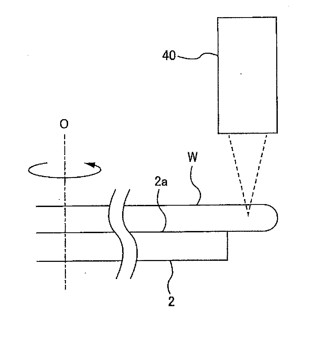
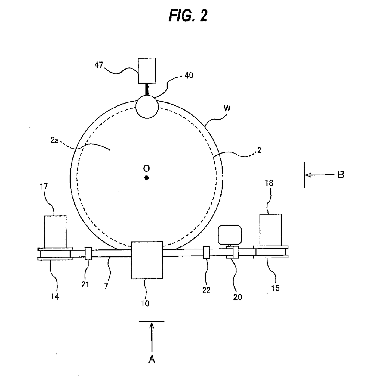
[0075]Embodiments will now be described with reference to the drawings.

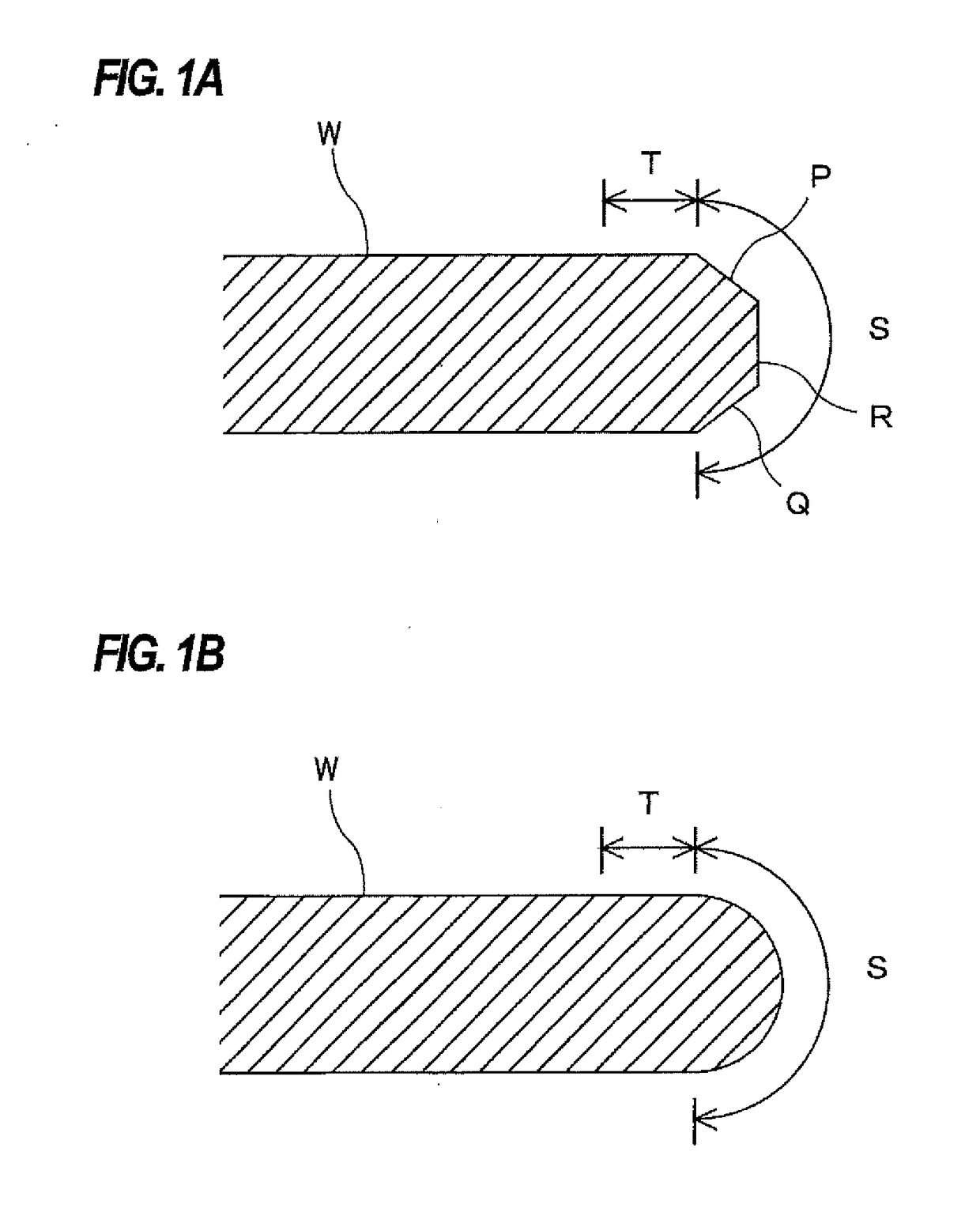
[0076]FIGS. 1A and 1B are enlarged cross-sectional views each showing a peripheral portion of a substrate (e.g., a wafer). More specifically, FIG. 1A is a cross sectional view of a substrate of a so-called straight type, and FIG. 1B is a cross sectional view of a substrate of a so-called round type. The peripheral portion of the substrate includes a bevel portion and an edge portion. In a substrate W shown in FIG. 1A, a bevel portion is an outermost circumferential surface (indicated by symbol S) including an upper slope (or an upper bevel portion) P, a lower slope (or a lower bevel portion) Q, and a side portion (or an apex) R of the substrate W. In a substrate W shown in FIG. 1B, a bevel portion is a portion (indicated by symbol S) constituting an outermost circumferential surface of the substrate W and having a curved cross section. The edge portion is a flat portion T located radially inwardly of the bevel po...


PUM

PropertyMeasurementUnit
thicknessaaaaaaaaaa
angleaaaaaaaaaa
pressing forceaaaaaaaaaa

Abstract

A method and an apparatus for processing a peripheral portion of a substrate, such as a wafer, are disclosed. The substrate processing method includes: holding a substrate on a substrate stage; rotating the substrate stage and the substrate about an axis of the substrate stage; directing a laser beam to an edge portion of the rotating substrate to form an annular crack in the substrate; and pressing a polishing tool against the edge portion of the rotating substrate to form a stepped recess in a peripheral portion of the substrate.

Description

CROSS REFERENCE TO RELATED APPLICATION[0001]This application claims priority to U.S. Provisional Patent Application No. 62 / 395,068 filed Sep. 15, 2016, the entire contents of which are hereby incorporated by reference.BACKGROUND[0002]Control of a surface condition of a wafer has recently attracted attention from the viewpoint of an increase in a yield in manufacturing of semiconductor devices. In a semiconductor device manufacturing process, films of various materials are formed on a silicon substrate. Therefore, an unnecessary film(s) or surface roughness is formed on a peripheral portion of the substrate. These days it is a common practice to transport a substrate while holding only a peripheral portion of the substrate with arms. With such a background, an unnecessary film, remaining on a peripheral portion of a substrate, may peel off during various processes and may adhere to a device formed on the substrate, resulting in reduced yield. Thus, in order to remove an unnecessary f...

Claims


Application Information

Patent Timeline
Patent Type & Authority Applications(United States)
IPC IPC(8): H01L21/304B23K26/08
CPCH01L21/3043B23K2201/40B23K26/0823H01L21/304H01L21/02021H01L21/67138B24B21/002B24B21/004B24B21/08B24B9/065B23K2101/40B24B37/00
Inventor ITO, KENYASEKI, MASAYAKOBAYASHI, KENICHIYAMASHITA, MICHIYOSHI
Owner EBARA CORP
Why Eureka
Try Eureka