Display device and electronic device

Active Publication Date: 2018-04-12
SEMICON ENERGY LAB CO LTD
View PDF1 Cites 5 Cited by
  • Summary
  • Abstract
  • Description
  • Claims
  • Application Information

AI Technical Summary

Benefits of technology

[0007]In miniaturization of transistors, high mask alignment accuracy is required in a lithography process. In addition, a margin is required between patterns for a transistor on the assumption of mask misalignment, which makes it difficult to miniaturize transistors. Furthermore, a process flow becomes complicated when the number of lithog

Problems solved by technology

In addition, a margin is required between patterns for a transistor on the assumption of mask misalignment, which makes it difficult to miniaturize transistors.
Furthermore, a process flow becomes complicated when the number of lithography processes is large, resulting in a reduction in

Method used


Image

  • Display device and electronic device
  • Display device and electronic device
  • Display device and electronic device

Examples


Example

Embodiment 1

[0126]In this embodiment, display devices of one embodiment of the present invention and methods for manufacturing the display devices will be described with reference to FIGS. 1A to 1C to FIGS. 46A to 46D.

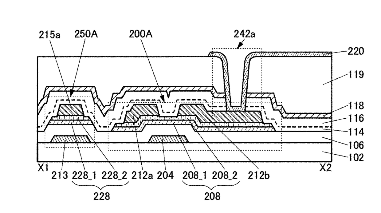
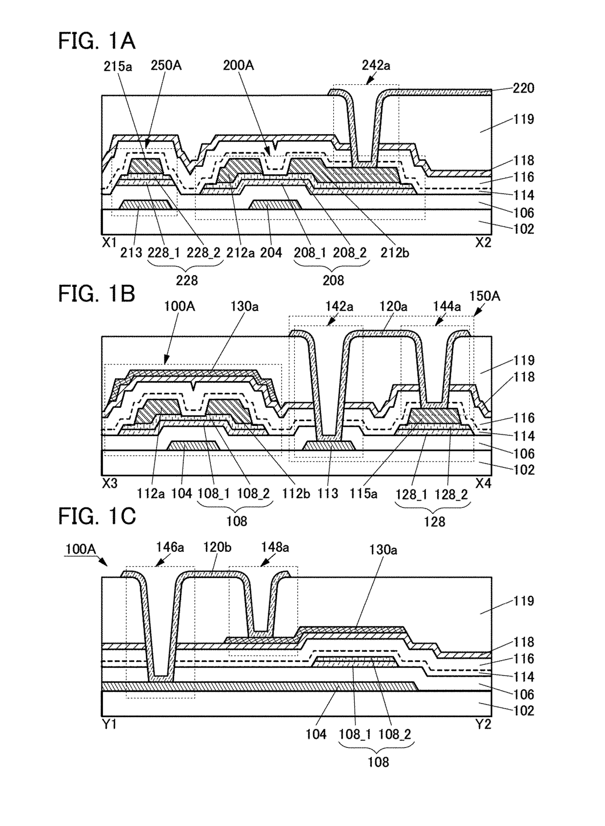
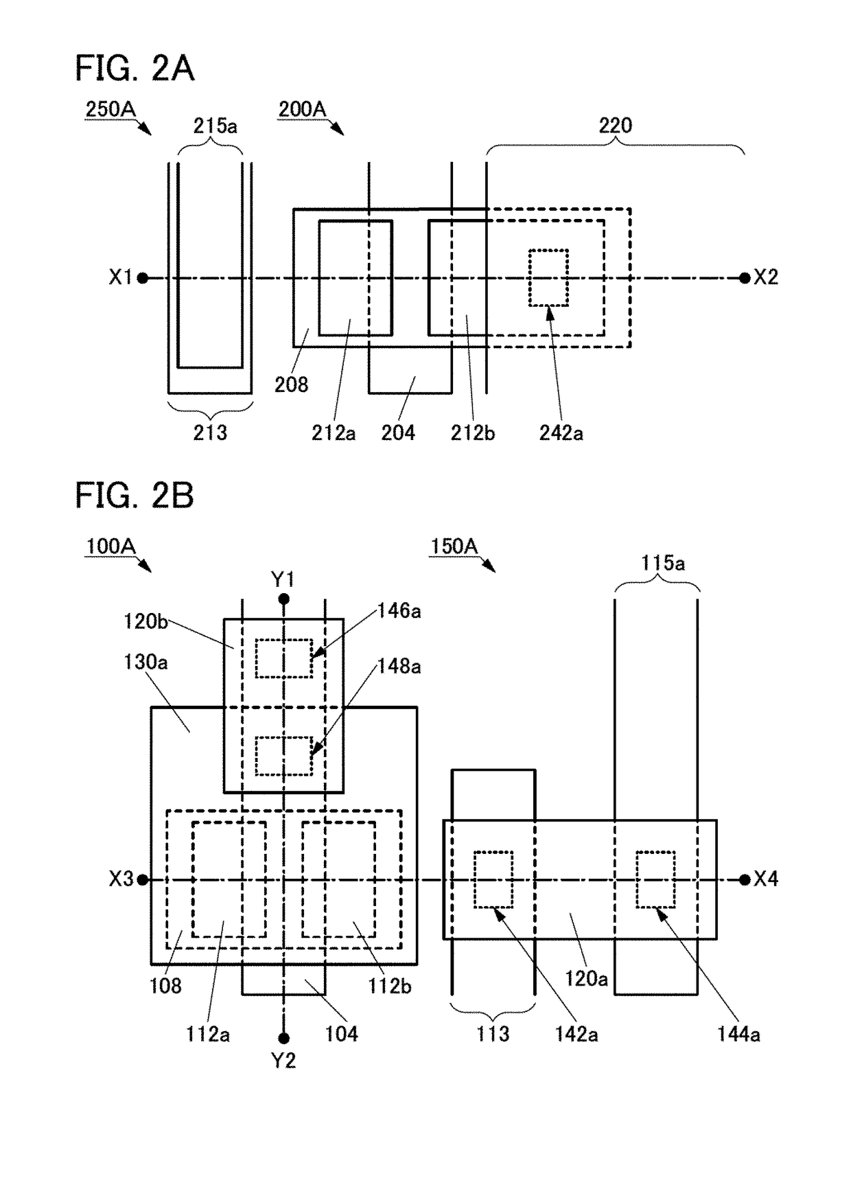
[0127]FIGS. 1A to 1C are cross-sectional views of transistors in a pixel portion and a driver circuit included in a display device of one embodiment of the present invention. FIGS. 2A and 2B are top views of the transistors.

[0128]The display device of one embodiment of the present invention includes a transistor 100A, a transistor 200A, a capacitor 250A, and a connection portion 150A.

[0129]FIG. 1A is a cross-sectional view of the transistor 200A and the capacitor 250A included in the pixel portion, which corresponds to a cross-sectional view taken along dashed-dotted line X1-X2 in FIG. 2A. FIG. 1B is a cross-sectional view of the transistor 100A and the connection portion 150A included in the driver circuit, which corresponds to a cross-sectional view taken along dashe...

Example

Embodiment 2

[0511]In this embodiment, the metal oxide film of one embodiment of the present invention will be described with reference to FIG. 47, FIG. 48, FIGS. 49A to 49L, and FIGS. 50A to 50C.

[0512]Described below is the detail of a metal oxide having a CAC composition that can be used in the transistor disclosed in one embodiment of the present invention. As a typical example of the metal oxide having a CAC composition, a CAC-OS will be described here.

[0513]In the CAC-OS, as illustrated in FIG. 47 for example, elements contained in the metal oxide are unevenly distributed to form the regions 001 and 002 each containing any of the elements as a main component. The regions are mixed to form or to be distributed in a mosaic pattern. In other words, the CAC-OS has a composition in which elements included in a metal oxide are unevenly distributed. Materials including unevenly distributed elements each have a size greater than or equal to 0.5 nm and less than or equal to 10 nm, prefer...

Example

Embodiment 3

[0578]In this embodiment, examples of a display device that includes the transistor described in the above embodiments are described below with reference to FIG. 51 to FIG. 63.

[0579]FIG. 51 is a top view illustrating an example of a display device. A display device 700 in FIG. 51 includes a pixel portion 702 provided over a first substrate 701, a source driver circuit portion 704 and a gate driver circuit portion 706 that are provided over the first substrate 701, a sealant 712 provided to surround the pixel portion 702, the source driver circuit portion 704, and the gate driver circuit portion 706, and a second substrate 705 provided to face the first substrate 701. The first substrate 701 and the second substrate 705 are sealed with the sealant 712. That is, the pixel portion 702, the source driver circuit portion 704, and the gate driver circuit portion 706 are enclosed by the first substrate 701, the sealant 712, and the second substrate 705. Although not illustrated...


PUM


Abstract

The number of lithography processes is reduced and a high-definition display device is provided. The display device includes a pixel portion and a driver circuit for driving the pixel portion. The pixel portion includes a first transistor and a pixel electrode electrically connected to the first transistor. The driver circuit includes a second transistor and a connection portion. The second transistor includes a metal oxide film, first and second gate electrodes that face each other with the metal oxide film positioned therebetween, source and drain electrodes over and in contact with the metal oxide film, and a first wiring connecting the first and second gate electrodes. The connection portion includes a second wiring on the same surface as the first gate electrode, a third wiring on the same surface as the source electrode and the drain electrode, and a fourth wiring connecting the second wiring and the third wiring. The pixel electrode, the first wiring, and the fourth wiring are formed using the same layer.

Description

BACKGROUND OF THE INVENTION1. Field of the Invention[0001]One embodiment of the present invention relates to a display device and an electronic device.[0002]Note that one embodiment of the present invention is not limited to the above technical field. The technical field of one embodiment of the invention disclosed in this specification and the like relates to an object, a method, or a manufacturing method. One embodiment of the present invention relates to a process, a machine, manufacture, or a composition of matter. In particular, one embodiment of the present invention relates to a semiconductor device, a display device, a light-emitting device, a power storage device, a memory device, a driving method thereof, or a manufacturing method thereof.[0003]In this specification and the like, a semiconductor device generally means a device that can function by utilizing semiconductor characteristics. A semiconductor element such as a transistor, a semiconductor circuit, an arithmetic d...

Claims


Application Information

Patent Timeline
IPC IPC(8): G09G3/30H01L27/32H01L29/786H01L29/417
CPCG09G3/30H01L27/3244H01L29/78693H01L29/78696H01L29/41733G09G2330/021G09G3/3659G09G3/3677G09G3/3688H01L29/66969H01L29/7869H01L27/1225H01L27/1288H10K59/1213H10K59/131H10K59/1201H10K59/35H10K59/123H10K59/12
Inventor KATAYAMA, MASAHIROKUROSAKI, DAISUKEOKAZAKI, KENICHIKOEZUKA, JUNICHI
Owner SEMICON ENERGY LAB CO LTD
Why Eureka
Try Eureka