Non-volatile memory
- Summary
- Abstract
- Description
- Claims
- Application Information
AI Technical Summary
Benefits of technology
Problems solved by technology
Method used
Image
Examples
Embodiment Construction
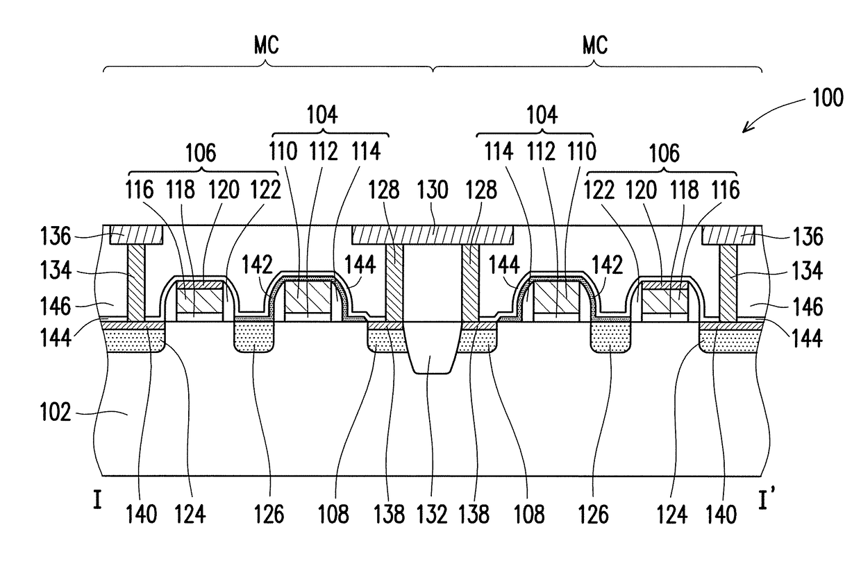
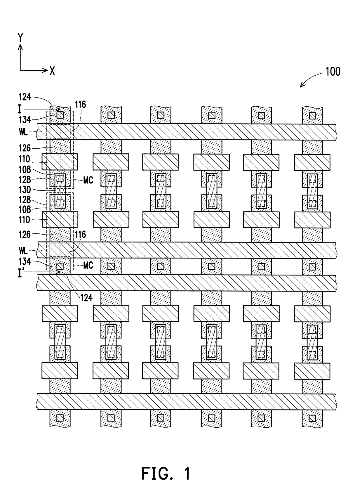
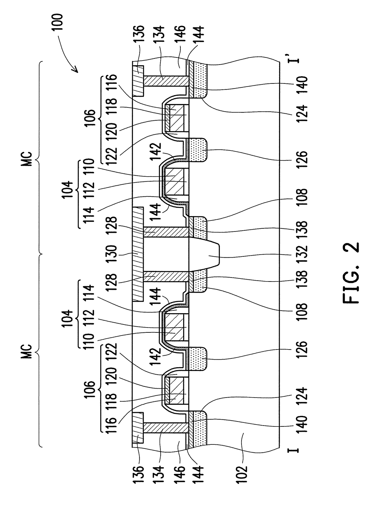
[0032]FIG. 1 is a top view of a non-volatile memory of an embodiment of the invention. FIG. 2 is a cross-section along section line I-I′ in FIG. 1. FIG. 1 omits some of the components in FIG. 2 to more clearly show the relationships between the other components.
[0033]Referring to both FIG. 1 and FIG. 2, a non-volatile memory 100 includes memory cells MC. Each of the memory cells MC includes a substrate 102, a floating gate structure 104, a select gate structure 106, and a doped region 108. The non-volatile memory 100 is, for instance, a NOR-type non-volatile memory. The substrate 102 is, for instance, a silicon substrate. Moreover, the memory cells MC can share the substrate 102.
[0034]The floating gate structure 104 is disposed on the substrate 102. The floating gate structure 104 includes a floating gate 110 and a dielectric layer 112. The floating gate 110 is disposed on the substrate 102. The floating gate 110 is, for instance, a single doped polysilicon layer. The forming method...
PUM
 Abstract
Description
Claims
Application Information


