Elastic wave device

a technology of elastic wave and thin film, applied in the direction of impedence networks, electrical devices, etc., can solve the problems of difficult easy interfacial peeling in multi-layer film, etc., to reduce or prevent cracking and chipping of piezoelectric thin film, the effect of low acoustic impedan

Active Publication Date: 2018-04-12
MURATA MFG CO LTD
View PDF4 Cites 6 Cited by
  • Summary
  • Abstract
  • Description
  • Claims
  • Application Information

AI Technical Summary

Benefits of technology

[0014]In an elastic wave device according to a preferred embodiment of the present invention, a second wiring electrode which is electrically connected to the interdigital transducer electrode and which extends from a location on the piezoelectric thin film to a location on the insulating layer is further included, wherein at least a portion of the second support layer is disposed on the second wiring electrode. With this configuration, three-dimensional wiring of the wire disposed on the piezoelectric thin film and the second wiring electrode are able to be constructed, and the productivity is improved.
[0022]In the elastic wave devices according to various preferred embodiments of the present invention, cracking and chipping of the piezoelectric thin film is reduced or prevented, and interfacial peeling in the multilayer film and between the multilayer film and the piezoelectric thin film does not easily occur. In addition, the strength of the elastic wave devices is able to be improved.

Problems solved by technology

With this configuration, interfacial peeling does not easily occur in the multilayer film.
With this configuration, when an external connection terminal is disposed, cracking and chipping of a piezoelectric thin film do not easily occur even if a force is applied to the first support layer.

Method used


Image

  • Elastic wave device
  • Elastic wave device
  • Elastic wave device

Examples


Embodiment Construction

[0033]The specific preferred embodiments of the present invention will be described below with reference to the drawings so as to clarify the present invention.

[0034]In this regard, it is indicated that each of the preferred embodiments described in the present specification is an exemplification and that the configuration may be partially replaced or combined with the configuration of another preferred embodiment.

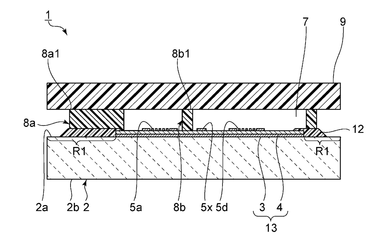
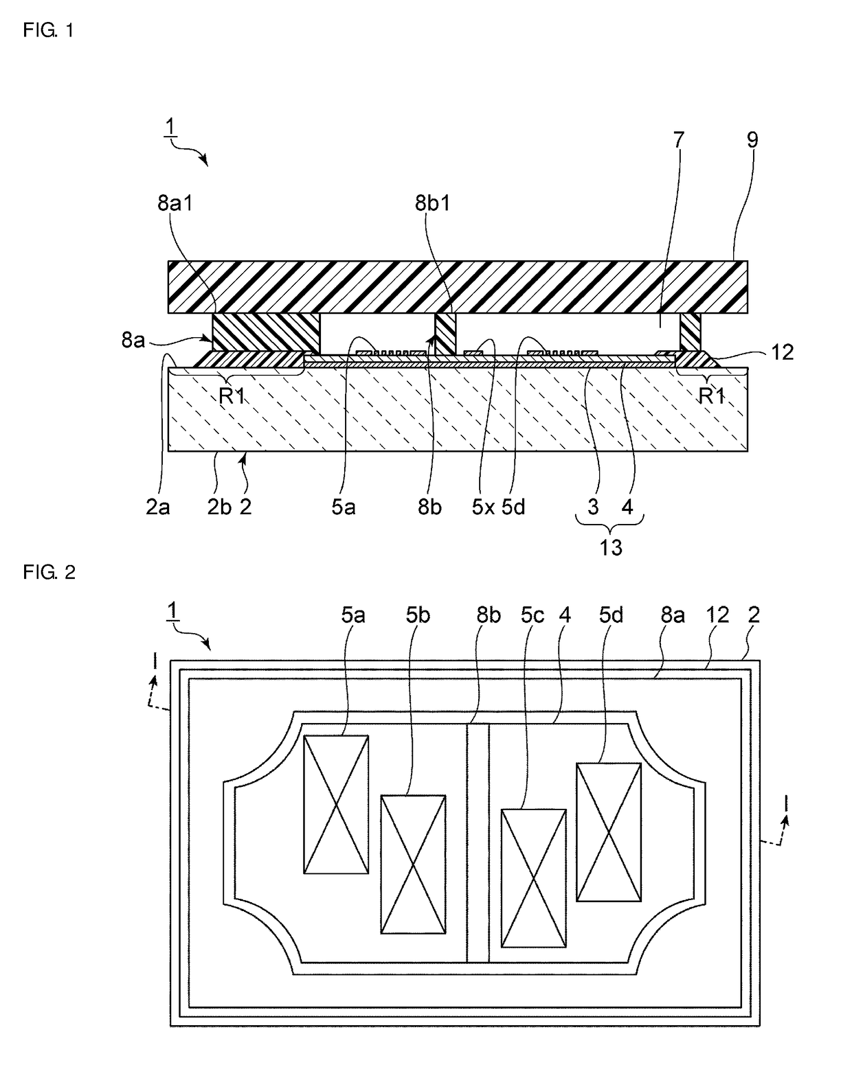
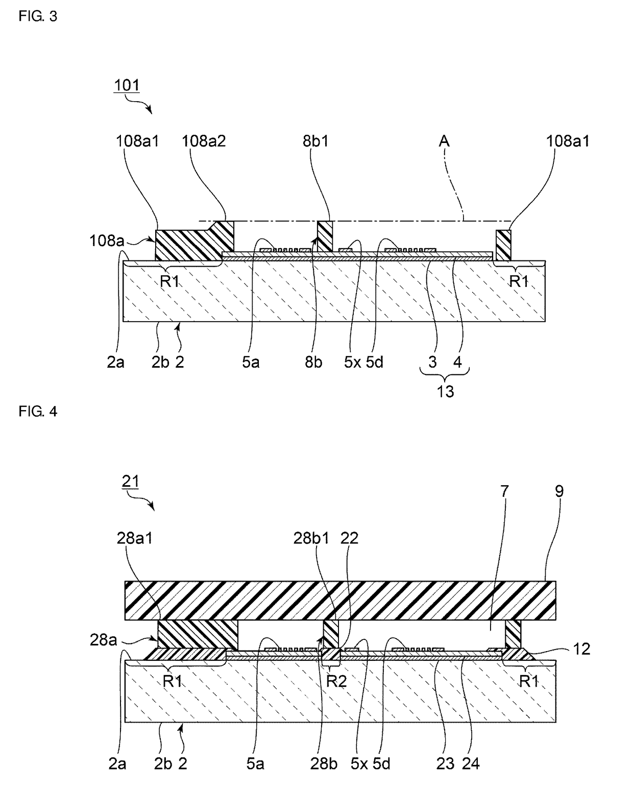
[0035]FIG. 1 is a sectional view of an elastic wave device according to a first preferred embodiment of the present invention, along line I-I in FIG. 2 described later.

[0036]An elastic wave device 1 includes a support substrate 2. The support substrate 2 includes a first principal surface 2a and a second principal surface 2b which are opposite to each other. A multilayer film 13 is disposed on the first principal surface 2a. More specifically, the multilayer film 13 includes a piezoelectric thin film 4 and a low acoustic velocity film 3 as a layer other than the piezoelect...


PUM


Abstract

An elastic wave device includes a multilayer film stacked on a support substrate. A first support layer surrounds a region including interdigital transducer electrodes. A second support layer is disposed in the region surrounded by the first support layer. A cover is fixed on the first support layer and the second support layer so as to close a cavity defined by the first support layer. The multilayer film is partially disposed on the support substrate, and an insulating layer is disposed in at least a portion of a region in which the multilayer film is not disposed. At least one of the first support layer and the second support layer is disposed on the insulating layer.

Description

CROSS REFERENCE TO RELATED APPLICATIONS[0001]This application claims the benefit of priority to Japanese Patent Application No. 2015-127147 filed on Jun. 25, 2015 and is a Continuation Application of PCT Application No. PCT / JP2016 / 067407 filed on Jun. 10, 2016. The entire contents of each application are hereby incorporated herein by reference.BACKGROUND OF THE INVENTION1. Field of the Invention[0002]The present invention relates to an elastic wave device in which a multilayer film including a piezoelectric thin film is stacked on a support substrate.2. Description of the Related Art[0003]In an elastic wave device according to International Publication WO2012 / 086639A1, a multilayer film is disposed on a support substrate, and a piezoelectric thin film is stacked on the multilayer film. The multilayer film includes a high acoustic velocity film and a low acoustic velocity film. The low acoustic velocity film is made of a film through which a bulk wave propagates at an acoustic veloci...

Claims


Application Information

Patent Timeline
Patent Type & Authority Applications(United States)
IPC IPC(8): H03H9/10H03H9/02H03H9/205
CPCH03H9/1071H03H9/02984H03H9/02574H03H9/205H03H9/02992H03H9/02897H03H9/25H03H9/125
Inventor FUKUSHIMA, MASAHIROKAI, SEIJIKOYANAGI, TAKUYA
Owner MURATA MFG CO LTD
Why Eureka
Try Eureka