
Optical inspection apparatus and method and method of fabricating semiconductor device using the apparatus

a technology of optical inspection and semiconductor devices, applied in semiconductor/solid-state device testing/measurement, material analysis using wave/particle radiation, instruments, etc., can solve the problems of difficult to obtain thickness information in a wide region of interest, take a long time to obtain thickness information, etc., to improve the reliability of semiconductor devices and yield semiconductor processes. , the effect of high precision

Inactive Publication Date: 2018-05-24
SAMSUNG ELECTRONICS CO LTD
View PDF6 Cites 4 Cited by
  • Summary
  • Abstract
  • Description
  • Claims
  • Application Information

AI Technical Summary

Benefits of technology

The patent describes an optical inspection apparatus and method that can inspect thickness information of an entire region of interest (ROI) with high precision. This can improve the reliability and yield of semiconductor devices, and the method includes generating 2D images of the inspection target in multiple wavelength regions using a broadband light source, monochromator, and image obtaining apparatus, and analyzing these images using analysis device. The image obtaining apparatus allows the light to be incident on the inspection target without a beam splitter, reflected by the target, and generate 2D images.

Problems solved by technology

However, it may be difficult to obtain thickness information of a wide region of interest (ROI).
Also, even if it is possible to obtain thickness information of the ROI, it may take a long time to obtain the thickness information.

Method used


Image

  • Optical inspection apparatus and method and method of fabricating semiconductor device using the apparatus
  • Optical inspection apparatus and method and method of fabricating semiconductor device using the apparatus
  • Optical inspection apparatus and method and method of fabricating semiconductor device using the apparatus

Examples


Embodiment Construction

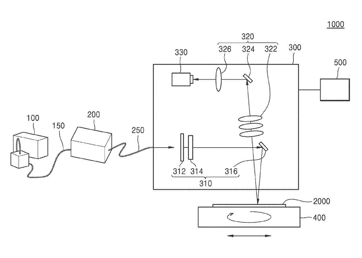
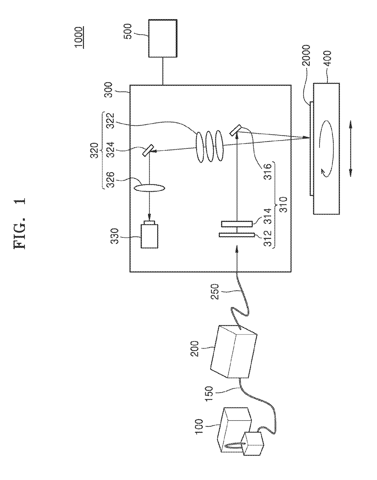
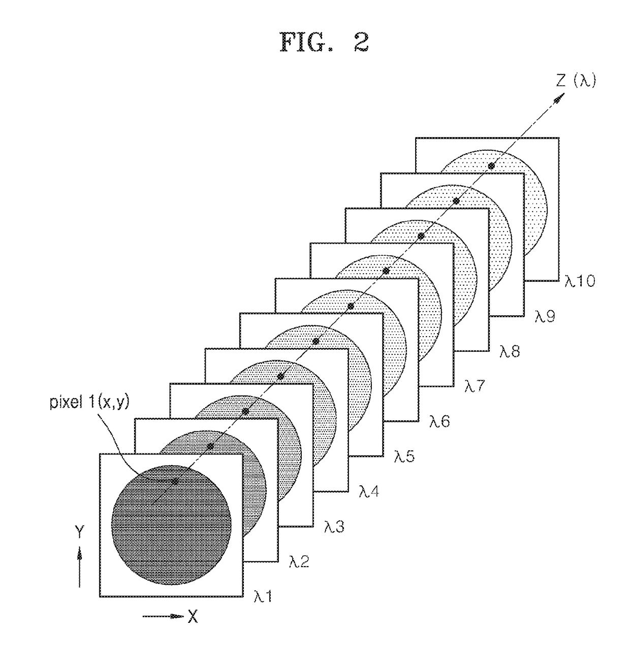
[0025]FIG. 1 is a schematic diagram showing the configuration of an optical inspection apparatus 1000 according to an example embodiment of the inventive concept, and FIG. 2 is a schematic diagram of two-dimensional (2D) images relative to a wavelength obtained by the optical inspection apparatus 1000 of FIG. 1.

[0026]Referring to FIG. 1, the optical inspection apparatus 1000 according to the present embodiment includes a light source 100, a monochromator 200, an image obtaining apparatus 300, a stage 400, and an analysis device 500.

[0027]In an example embodiment, the light source 100 is a broadband light source configured to generate and output broadband light. For example, in the optical inspection apparatus 1000 according to the present embodiment, the light source 100 may generate and output light having a band (e.g., wavelength) of about (or exactly) 170 nm to about (or exactly) 2100 nm. The light source 100 may be configured as a broadband light source and provide light of vari...


PUM


Abstract

An optical inspection apparatus includes a broadband light source, a monochromator, an image obtaining apparatus, and an analysis device. The monochromator is configured to convert light from the broadband light source into a plurality of monochromatic beams of different wavelengths and sequentially output the monochromatic beams, where each beam has a preset wavelength width and corresponds to one of a plurality of different wavelength regions. The image obtaining apparatus is configured to allow each monochromatic beam output from the monochromator to be incident to a top surface of an inspection target without using a beam splitter, allow light reflected by the inspection target to travel in a form of light of an infinite light source, and generate 2D images of the inspection target. The analysis device is configured to analyze the 2D images of the inspection target in the plurality of wavelength regions.

Description

CROSS-REFERENCE TO RELATED APPLICATION[0001]This application claims the benefit of and priority to Korean Patent Application No. 10-2016-0156594, filed on Nov. 23, 2016, in the Korean Intellectual Property Office, the disclosure of which is incorporated by reference in its entirety herein.BACKGROUND1. Technical Field[0002]The inventive concept relates to an optical inspection apparatus and method, and more particularly, to an optical inspection apparatus and method using spectral reflectometry (SR).2. Discussion of Related Art[0003]An SR technique is a technique of measuring a thickness and / or critical dimension (CD) of a thin film by using a phenomenon where wavelength characteristics of light reflected by the thin film are changed. When light is reflected by the thin film, reflectance may vary according to wavelength due to interference between light beams reflected at interfacial surfaces. The SR technique may include applying broadband light to a specimen of a thin film, quantit...

Claims


Application Information

Patent Timeline
IPC IPC(8): H01L21/66H01L21/78G01B11/06G01B11/02G01N21/88G01N21/95
CPCH01L21/78G01B11/06G01N2021/8848H01L22/12G01N21/9501G01B11/022G01N21/8806G01B11/0633G01B2210/56G01N2021/8845H01L22/24G01N2223/315
Inventor KIM, YOUNG-DUKJEON, BYEONG-HWANKANG, KYUNG-SIKKO, KANG-WOONGKIM, SOO-RYONGKIM, TAE-JOONGPARK, JUN-BUMSONG, GIL-WOOJANG, SUNG-HOJEON, HYOUNG-JOJOO, JAE-CHOL
Owner SAMSUNG ELECTRONICS CO LTD
Learn More