

Packaging method of long-distance sensor
- Summary
- Abstract
- Description
- Claims
- Application Information
AI Technical Summary
Benefits of technology
Problems solved by technology
Method used
Image

Examples
Embodiment Construction
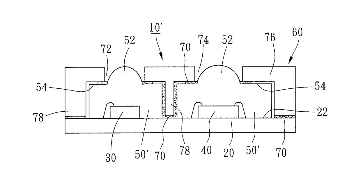
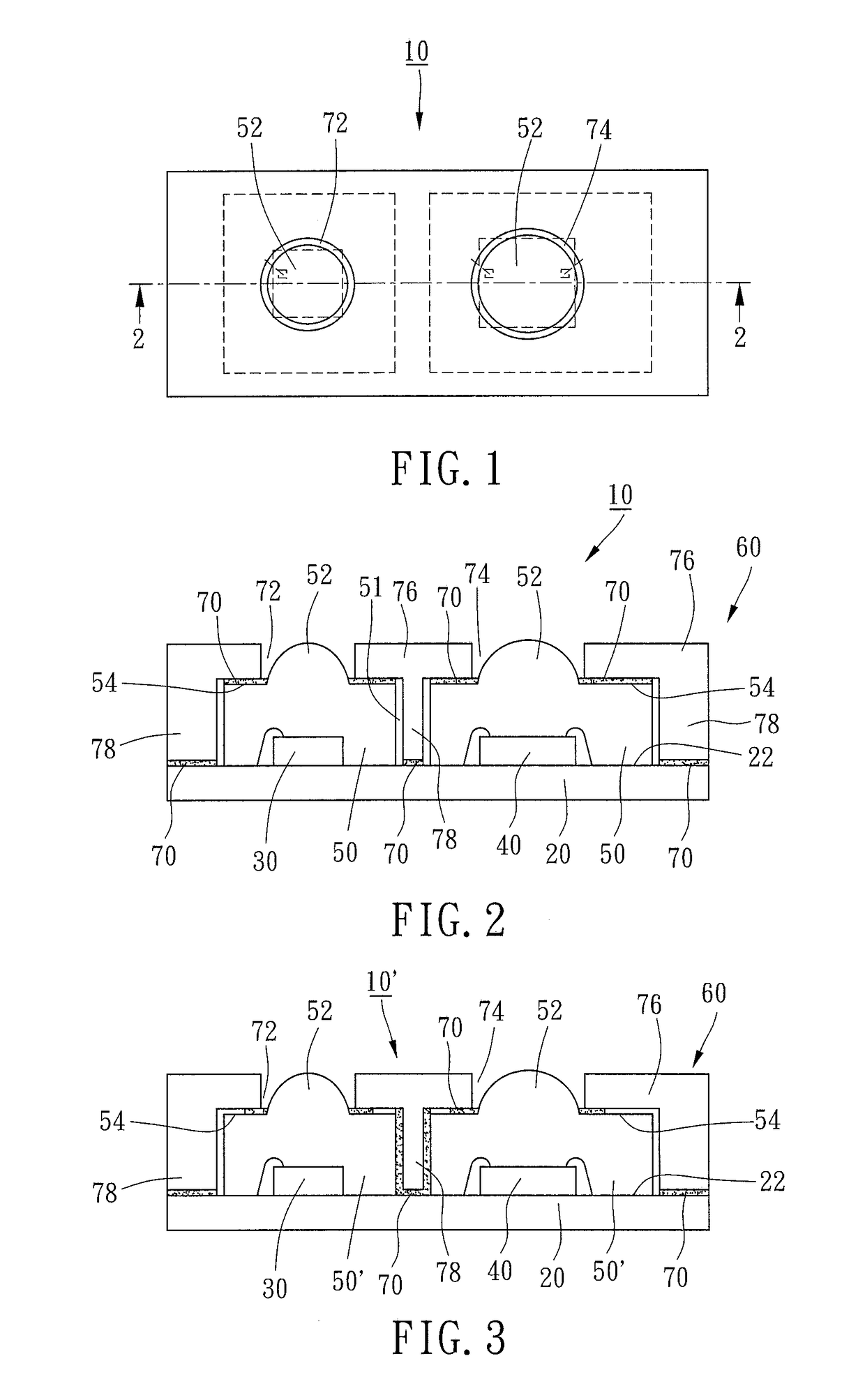
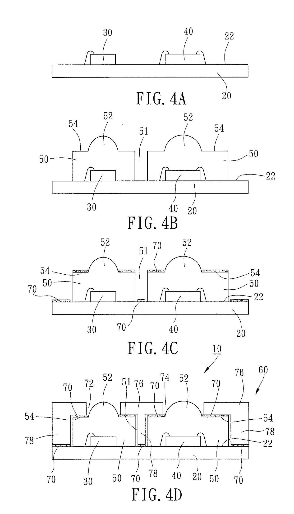
[0019]Referring to FIGS. 1-2, wherein a package structure 10 of a long-distance sensor according to a first preferred embodiment of the present invention is shown, the package structure 10 includes a substrate 20, a light-emitting chip 30, a sensing chip 40, two packaging gel bodies 50, and a cap 60.
[0020]The substrate 20 in this preferred embodiment may, but unlimited to, be a printed circuit board (usually referred to as “PCB”), a bismaleimide-triazine (usually referred to as “BT”) substrate, a glass fiber substrate (usually referred to as “FR4”), or a direct bonded copper (usually referred to as “DBC”) substrate. In this way, the manufacturing cost of the substrate 20 is relatively lower. The substrate 20 has a bearing surface 22.
[0021]The light-emitting chip 30 is disposed on the bearing surface 22, and may be electrically connected with the substrate 20 by wire bonding. In this preferred embodiment, the light-emitting chip 30 is an LED chip for emitting a light source.
[0022]The...
PUM
 Abstract
Description
Claims
Application Information