Fingerprint recognition apparatus
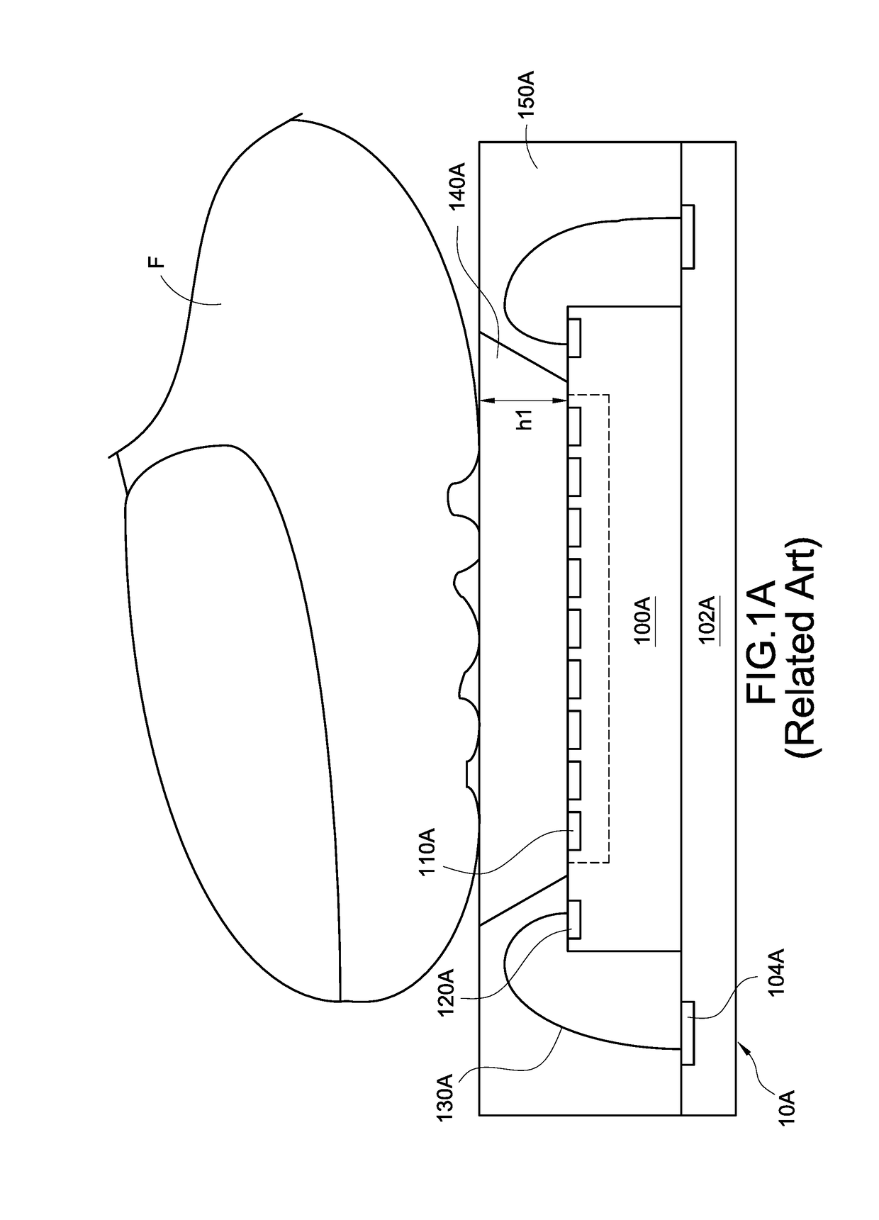
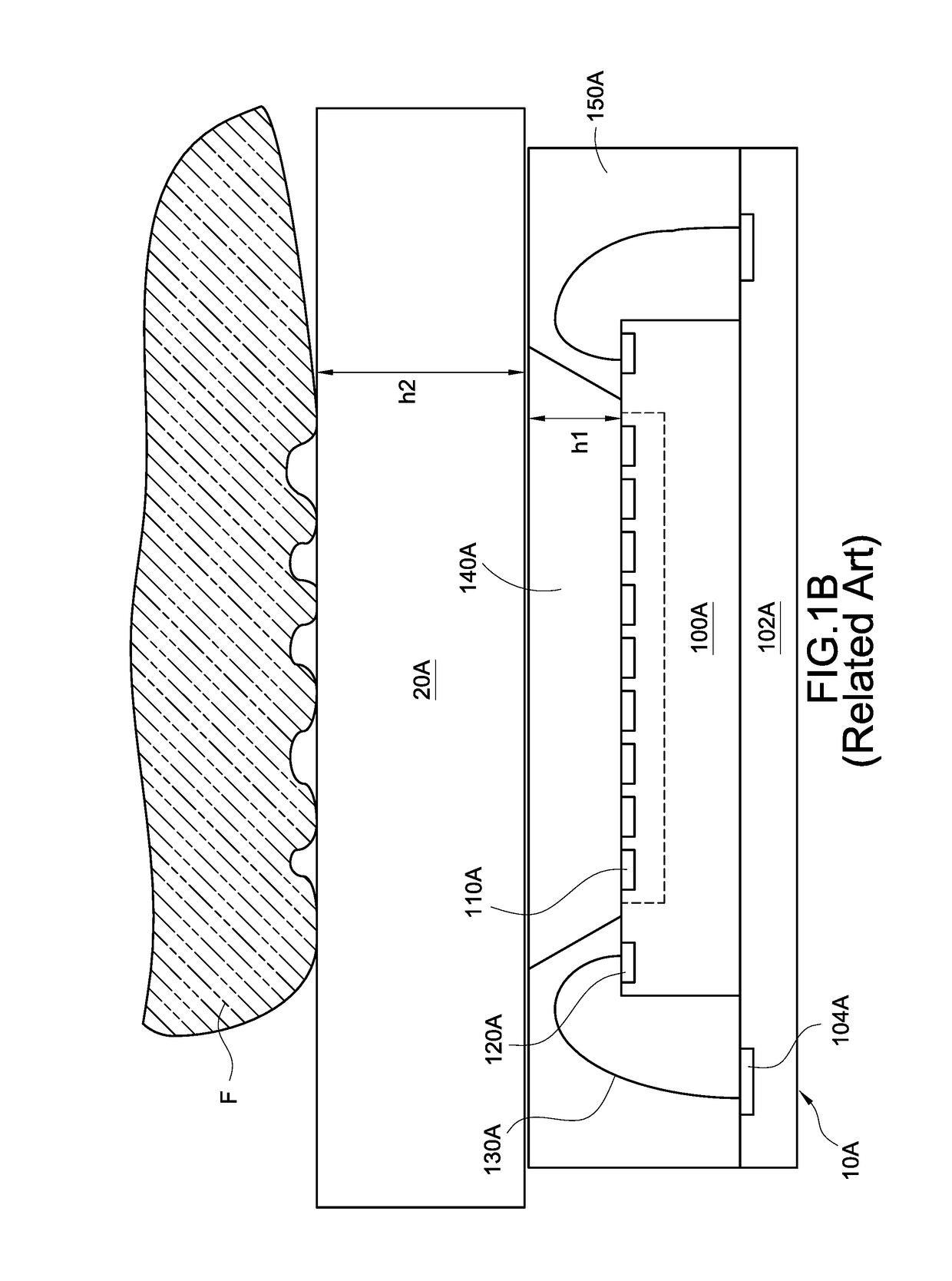
a fingerprint recognition and fingerprint technology, applied in the field of fingerprint recognition apparatus, can solve the problems of increasing cost, extra distance hb, and unable to integrate the capacitive fingerprint sensor below the protection glass
- Summary
- Abstract
- Description
- Claims
- Application Information
AI Technical Summary
Benefits of technology
Problems solved by technology
Method used
Image
Examples
first embodiment
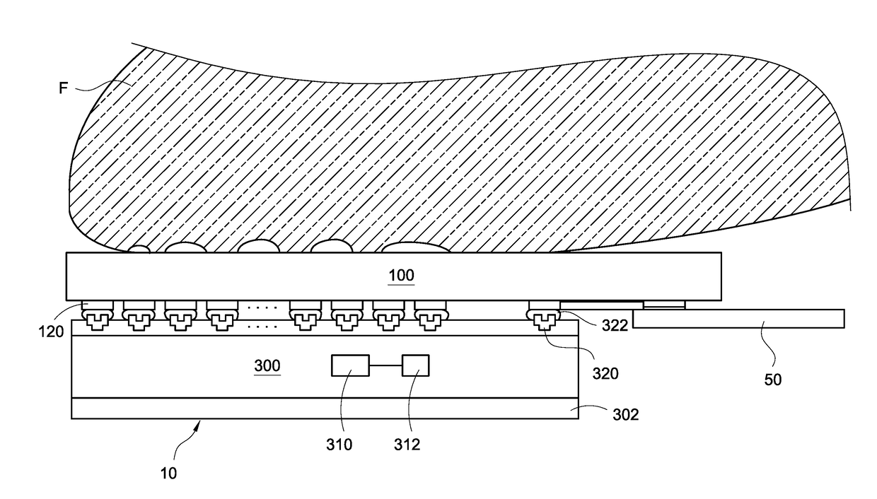
[0022]With reference to FIG. 3, the fingerprint recognition apparatus 10 is viewed from the finger pointing direction. The sensing electrodes 120 on the electrode-and-wiring substrate 100 are arranged, for example, in array manner. An area of each of the metal bumps 320 is not larger than an area of corresponding one of the sensing electrodes 120. Each of the sensing electrodes 120 is electrically connected with the fingerprint sensing circuit 310 of the IC chip 300 through the corresponding metal bumps 320. Moreover, the fingerprint sensing circuit 310 can be selectively connected with the sensing electrodes 120 through the connection of the metal bumps 320 and performs self-capacitance fingerprint sensing by sensing the detected signal respectively from the sensing electrodes 120. The technique of self-capacitance fingerprint sensing is well known art and is not detailed here for brevity. The metal bumps 320 can be formed by directly placing tin solder or gold on the electric pads...
fifth embodiment
[0026]FIG. 7 is a sectional view of the fingerprint recognition apparatus according to the present invention, and the embodiment shown in FIG. 7 is similar to that shown in FIG. 2. However, the external circuit board 50 shown in FIG. 2 is replaced by an electronic device 60 shown in FIG. 7. The electronic device 60 can be integrated circuit in COG or COF package. Moreover, even though not particularly illustrating, the top view for the embodiment shown in FIG. 7 can be referred to those shown in FIGS. 3 to 6. Therefore, further description regarding the embodiment in FIG. 7 is omitted here for brevity. In the embodiments shown in FIGS. 4 to 7, the electrode-and-wiring substrate 100 can be glass substrate (such as protection glass of display apparatus), ceramic substrate, sapphire substrate or polymer film. The thickness of the electrode-and-wiring substrate 100 can be reduced to several micro meters, which is one order of magnitude less than that of sealing resin 150A. The sealing r...
sixth embodiment
[0027]FIG. 8 is a sectional view of the fingerprint recognition apparatus according to the present invention, and the embodiment shown in FIG. 8 is similar to that shown in FIG. 2. However, the electrode-and-wiring substrate 100 shown in FIG. 2 is replaced by a wiring substrate 100′ shown in FIG. 8, and the IC chip 300 in FIG. 8 further comprising sensing electrodes 340. The sensing electrodes 340 can be implemented with the layout as the self-capacitance sensing electrodes shown in FIG. 3, the mutual-capacitance sensing electrodes shown in FIG. 4, or the mutual-capacitance sensing electrodes constituted by grouping a plurality of sensing electrodes as shown in FIG. 5. Similar to those embodiments shown in FIGS. 2-6, the wiring substrate 100′ further comprises a plurality of conductive pads 122 and a plurality of conductive wires 124. At least part of the conductive pads 122 are electrically connected with the conductive pads 52 of the external circuit board 50 and another part of t...
PUM
 Abstract
Description
Claims
Application Information


