Test architecture with an FPGA based test board to simulate a dut or end-point

a test board and test architecture technology, applied in the direction of measurement devices, error detection/correction, instruments, etc., can solve the problems of only testing duts in the system, critical time consumed replacing hardware bus adapter cards, and the number and type of duts that can be tested with a given ate body is limited, so as to achieve the effect of keeping the bandwidth requirements of the system bus

Active Publication Date: 2018-07-12
ADVANTEST CORP
View PDF8 Cites 35 Cited by
  • Summary
  • Abstract
  • Description
  • Claims
  • Application Information

AI Technical Summary

Benefits of technology

[0012]Accordingly, a need exists for a tester architecture that can address the problems with the systems described above. What is needed is a test architecture whereby the command and test pattern generation functionality can be transferred onto the FPGA, so that the processing load on the tester processor and the bandwidth requirements on the system bus can be kept at a minimum. This would be more efficient than prior configurations where the tester processor bore the entire processing load and the system bus conveyed test data and commands for all the DUTs connected to the ATE body. Further, what is needed is a test architecture whereby the communicative protocol engine can be programmed on FPGA devices so that the protocol used to communicate with the DUTs is reconfigurable.
[0013]In addition, what is needed is a tester system whereby the testing functionalities of the tester are reduced onto a small scale, small form factor, inexpensive test card or test board. This allows testing functionality and test development, e.g., test prototyping, to be performed easily on an engineer's bench top or lent or sold to a customer for test development. The small-scale test board or test card can also be fully software and hardware compatible with the larger tester systems. Accordingly, test development on the test card is readily portable to the larger systems.
[0014]Further, what is needed is a small scale test board that is also fully programmable and can be re-programmed to be an end-point to simulate a next generation device (or DUT), for instance. This provides an inexpensive way to re-purpose a miniature test card or board as a next generation device. With this small scale DUT emulator, the development of the tester for next generation devices can be readily completed.

Problems solved by technology

Because the tester processor, and not the FPGA, is responsible for generating the commands and test patterns, the number and type of DUTs that can be tested with a given ATE body is limited by the processing capabilities and programming of the tester processor.
Unless the PCIe hardware bus adapter cards are physically substituted with cards supporting the other protocol, such a system can only test DUTs that support the PCIe protocol.
Thus, on the test floor, critical time is consumed replacing hardware bus adapter cards when DUTs running a different protocol from the one that the existing adapter cards support need to be tested.
Another drawback of current tester systems is that the test systems tend to be large, cumbersome and cost-prohibitive.
While larger test systems may be ideal for testing in a production environment where a high volume of devices needs to be tested post-production, they are not ideal for development environments.
A further challenge associated with traditional tester systems is that they do not provide adequate functionality to enable a development engineer to test next generation devices that are not commercially available.
For example, if a next generation PCIe device or DUT is not yet commercially available, a development engineer would have no way of testing firmware or software being developed for the next generation device.
In other words, traditional tester systems do not provide functionality that allows a development engineer to readily develop and test firmware or software targeted towards yet to be produced next generation devices.

Method used


Image

  • Test architecture with an FPGA based test board to simulate a dut or end-point
  • Test architecture with an FPGA based test board to simulate a dut or end-point
  • Test architecture with an FPGA based test board to simulate a dut or end-point

Examples


Embodiment Construction

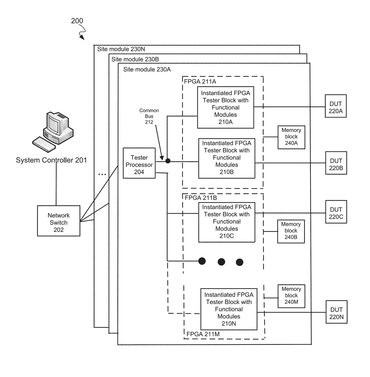
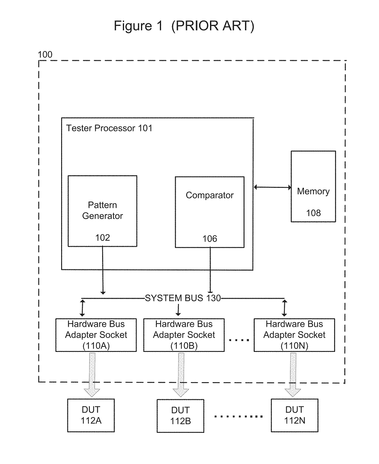
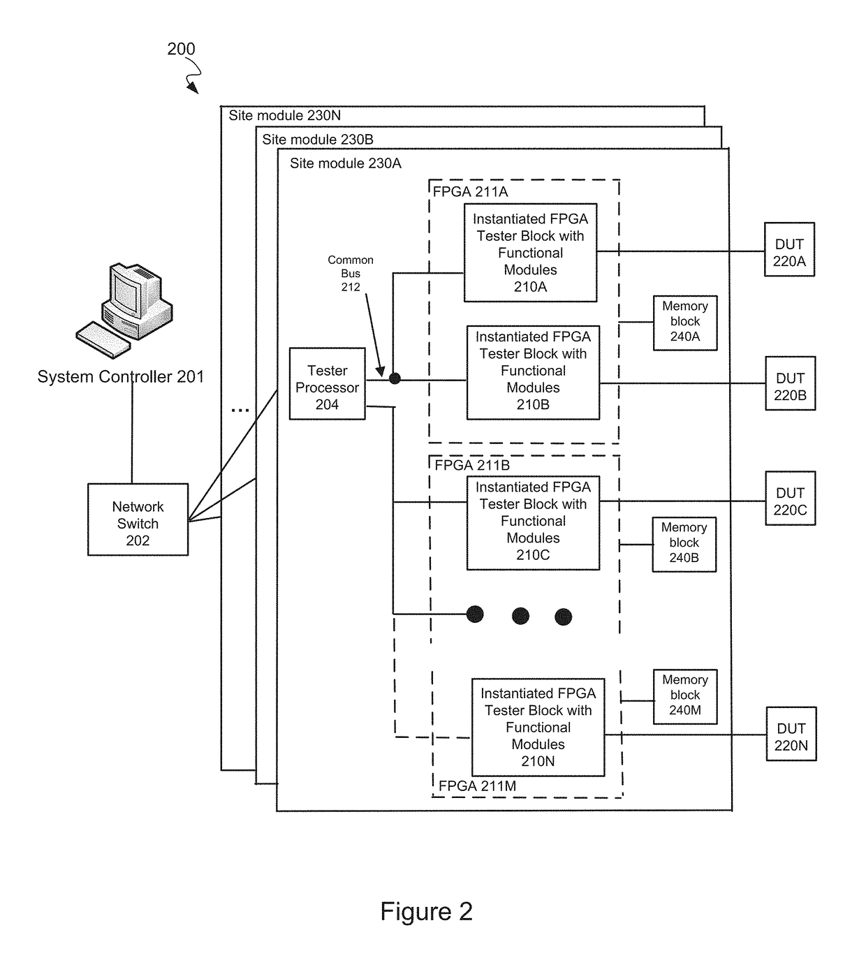
[0036]Reference will now be made in detail to embodiments, examples of which are illustrated in the accompanying drawings. While the embodiments will be described in conjunction with the drawings, it will be understood that they are not intended to limit the embodiments. On the contrary, the embodiments are intended to cover alternatives, modifications and equivalents. Furthermore, in the following detailed description, numerous specific details are set forth in order to provide a thorough understanding. However, it will be recognized by one of ordinary skill in the art that the embodiments may be practiced without these specific details. In other instances, well-known methods, procedures, components, and circuits have not been described in detail as not to unnecessarily obscure aspects of the embodiments.

Notation and Nomenclature Section

[0037]Some regions of the detailed descriptions which follow are presented in terms of procedures, logic blocks, processing and other symbolic repr...


PUM


Abstract

An automated test equipment (ATE) system capable of performing a test of semiconductor devices is presented. The system comprises a first test board including a first FPGA communicatively coupled to a controller via an interface board, wherein the first FPGA comprises a first core programmed to implement a communication protocol, and further wherein the FPGA is programmed with at least one hardware accelerator circuit operable to internally generate commands and data for testing a DUT. The system also includes a second test board comprising a second FPGA communicatively coupled to the first test board, wherein the second FPGA comprises a second core programmed to implement a communication protocol for a device under test, wherein the second FPGA is further programmed to simulate a DUT, and wherein the first FPGA is operable to communicate with the second FPGA in order to test a communication link between the first test board and the second test board.

Description

CROSS-REFERENCE TO RELATED APPLICATIONSRelated Applications[0001]The present application is a continuation-in-part of U.S. patent application Ser. No. 13 / 773,569, filed Feb. 21, 2013, entitled “A TEST ARCHITECTURE HAVING MULTIPLE FPGA BASED HARDWARE ACCELERATOR BLOCKS FOR TESTING MULTIPLE DUTS INDEPENDENTLY,” naming Gerald Chan, Eric Kushnick, Mei-Mei Su and Andrew Niemic as inventors, and having attorney docket number ATST-JP0090. That application is incorporated herein by reference in its entirety and for all purposes.FIELD OF THE INVENTION[0002]The present disclosure relates generally to the field of electronic device testing systems and more specifically to the field of electronic device testing equipment for testing devices under test (DUTs).BACKGROUND OF THE INVENTION[0003]Automated test equipment (ATE) can be any testing assembly that performs a test on a semiconductor device or electronic assembly. ATE assemblies may be used to execute automated tests that quickly perform me...

Claims


Application Information

Patent Timeline
Patent Type & Authority Applications(United States)
IPC IPC(8): G01R31/317
CPCG01R31/31724G01R31/31723G01R31/2601G01R31/31907G01R31/31908G06F11/263G01R31/31903G01R31/31919G01R35/00
Inventor CHAMPOUX, DUANESU, MEI-MEI
Owner ADVANTEST CORP
Why Eureka
Try Eureka