Display device

Active Publication Date: 2018-07-19
JAPAN DISPLAY INC
View PDF6 Cites 0 Cited by
  • Summary
  • Abstract
  • Description
  • Claims
  • Application Information

AI Technical Summary

Benefits of technology

The present invention solves the problem of degraded quality and reliability of flexible display devices when using polyimide substrates and oxide semiconductor TFTs due to the heat resistance of polyimide. The invention proposes a display device comprising a substrate formed by resin, an inorganic insulating film, and a thin film transistor including a semiconductor, wherein a reflectivity of infra-red light of a wave length of µm is 75% or more. This results in a flexible display device with high quality and high reliability.

Problems solved by technology

If the temperature goes over the glass transition temperature, the material itself gets damages, deceases a transparency, and consequently, a quality of the display is degraded.
If a silicon transistor is used for the TFT, even when the LTPS (Low Temperature Poly-Silicon) is used, the process temperature is higher than 400 centigrade, thus, it is difficult to use the polyimide for the substrate.

Method used


Image

  • Display device
  • Display device
  • Display device

Examples


first embodiment

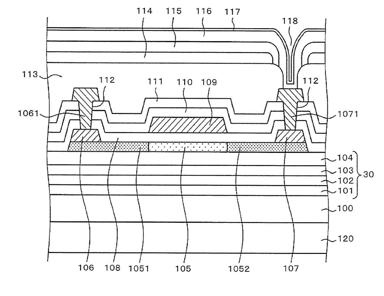
[0038]FIG. 1 is a plan view of a liquid crystal display device. In FIG. 1, the TFT substrate 100 and the counter substrate 200 adhere to each other via the seal material 150. The liquid crystal is sealed inwardly from the seal material 150. The display area 500 is formed inside of the seal material 150. In the display area 500 of FIG. 1, scanning lines 11 extend in lateral direction and arranged in longitudinal direction; the video signal lines 12 extend in longitudinal direction and arranged in lateral direction. A pixel 14 is formed in an area surrounded by the scanning lines 11 and the video signal lines 12.

[0039]The TFT substrate 100 is made bigger than the counter substrate 200; the portion where the TFT substrate 100 and the counter substrate 200 don't overlap is the terminal area, to which the flexible wiring substrate 1000 connects to supply powers and signals to the liquid crystal display device.

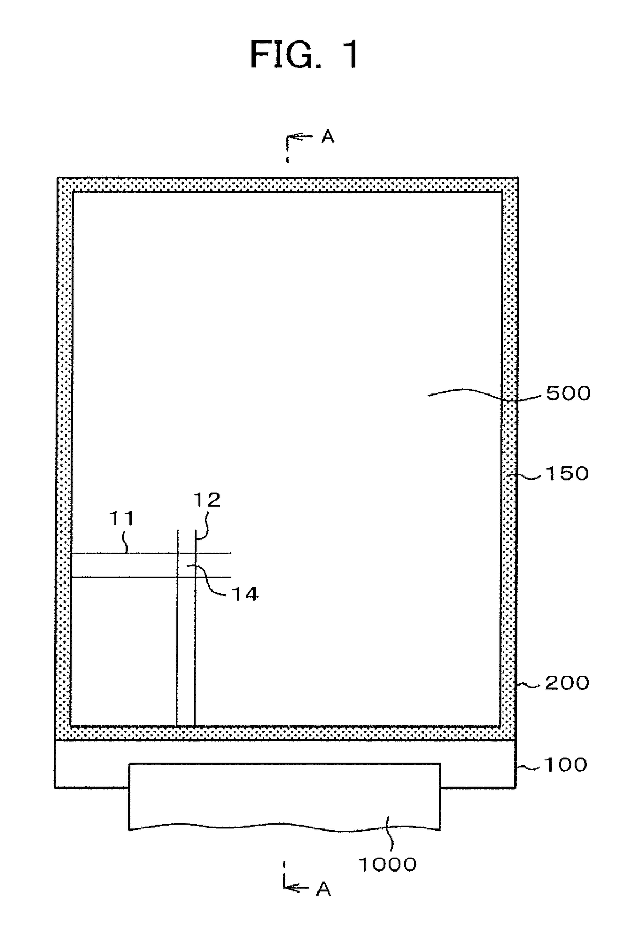
[0040]FIG. 2 is cross sectional view along the line A-A of FIG. 1. In FIG. 2, t...

second embodiment

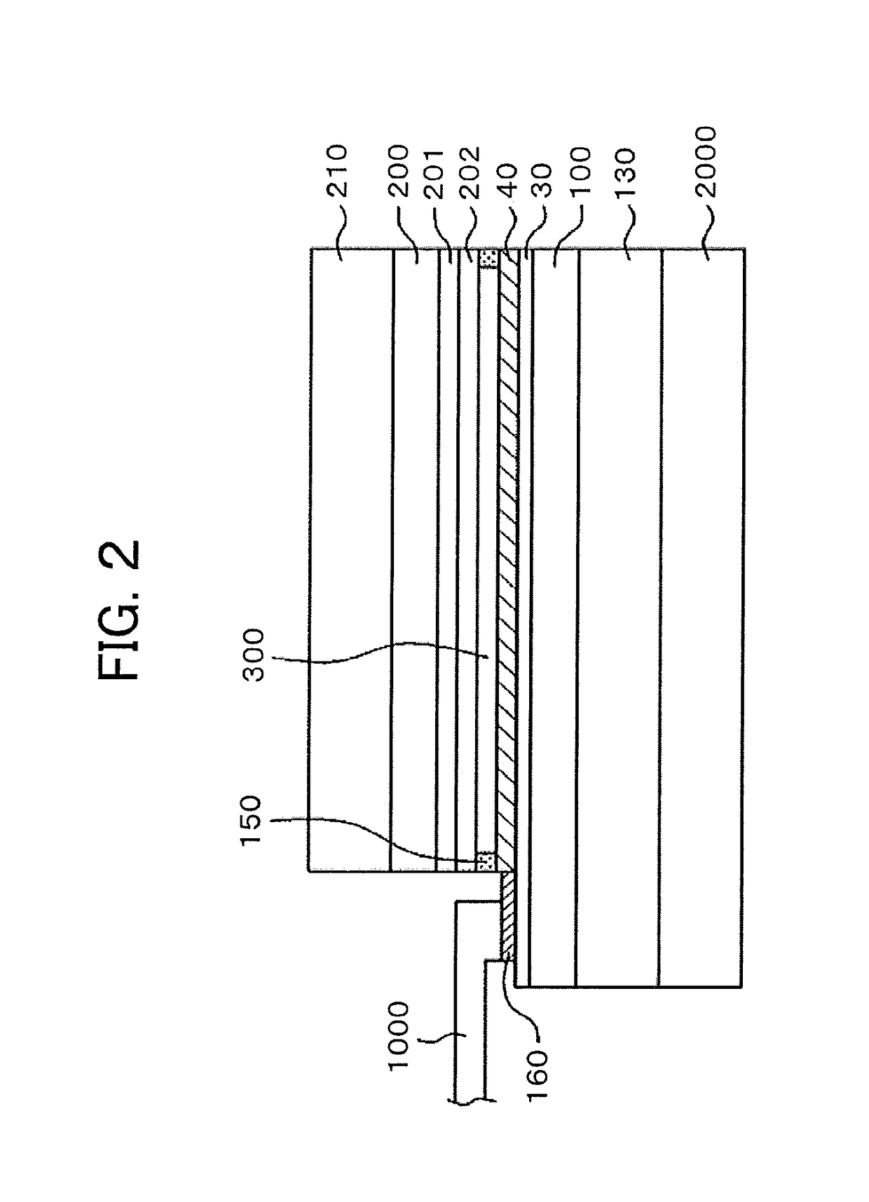
[0080]FIG. 18 is a cross sectional view of the structure of the TFT substrate according to the second embodiment. FIG. 18 differs from FIG. 12 of the first embodiment in that the second infra-red light reflection film 50 is formed between the third undercoat 103 and the fourth undercoat 104. The second infra-red light reflection film 50 overlaps at least with the oxide semiconductor 105 in a plan view. However, the second infra-red light reflection film 50 doesn't need to cover all the display area in FIG. 18. The second infra-red light reflection film 50 can be a metal as far as the absorbance in the infra-red light area is low. In this embodiment, an Al film of a thickness of 200 nm is used for the second infra-red light reflection film 50, which has an absorbance of 0.1 or less to the infra-red light of wave length of 2 μm, however, the thickness of the Al film can be changed in a range between 50 nm and 400 nm. If the thickness is less than 50 nm, the reflectivity decreases whil...

third embodiment

[0090]In the first embodiment and in the second embodiment, the present invention was explained in the case of the liquid crystal display device. The present invention is applicable to the organic EL display device, too. FIG. 21 is a plan view of the organic EL display device. In FIG. 21, the scanning lines 11 extend in lateral direction and arranged in longitudinal direction in the display area 500. A pairs of the video signal line 12 and the power line 13 extend in longitudinal direction and arranged in lateral direction. The pixel 14 is formed in the area surrounded by the scanning lines and pairs of the video signal line 12 and the power line 13. The scanning line driving circuit 501 is formed at both sides of the display area 500; the flexible wiring 1000 is connected to the terminal area to supply the power or the signals to the display device.

[0091]FIG. 22 is cross sectional view along the line B-B of FIG. 21. In FIG. 22, the TFT substrate is formed by the polyimide. The infr...


PUM


Abstract

The purpose of the present invention is to realize a flexible display includes a resin substrate and a TFT having an oxide. The structure of the invention is as follows. A display device comprising: a substrate formed by resin, an inorganic insulating film and a thin film transistor including a semiconductor, wherein an infra-red light reflecting film is formed between the substrate and the thin film transistor.

Description

CLAIM OF PRIORITY[0001]The present application claims priority from Japanese Patent Application JP 2017-005746 filed on Jan. 17, 2017, the content of which is hereby incorporated by reference into this application.BACKGROUND OF THE INVENTION(1) Field of the Invention[0002]The present invention relates to the display device having a resin substrate and Thin Film Transistors formed by oxide semiconductors.(2) Description of the Related Art[0003]The liquid crystal display device has a Thin Film Transistor (herein after TFT) in each of the pixels to control retrieving the data for the pixel. Sometimes, the built in driving circuit is made by TFTs.[0004]The organic EL display device has a first TFT and a second TFT in each of the pixels. The first TFT is a switching TFT that controls retrieving the data to the pixel. The second TFT is a driving TFT that controls the current to the light emitting element. Sometimes, the built in driving circuit is made by TFTs.[0005]Since a leak current i...

Claims


Application Information

Patent Timeline
IPC IPC(8): G02B5/20G02F1/1335G02F1/1368G02F1/1333H01L27/12H01L29/786H01L21/428
CPCG02B5/208G02F1/133509G02F1/1368G02F1/133305H01L27/1218H01L27/127H01L27/1262H01L27/1225H01L29/7869H01L29/78603H01L21/428H01L27/3262H01L51/0097G02F2001/13685G02F2203/11G02B5/26H01L29/78633H10K59/126H10K77/111G02F1/13685H10K59/1213
Inventor WATABE, KAZUFUMIKAWANAGO, HIROSHI
Owner JAPAN DISPLAY INC
Why Eureka
Try Eureka