Light-emitting diode structure, transfer assembly, and transfer method using the same

a technology of light-emitting diodes and assembly, applied in semiconductor devices, electrical equipment, semiconductor/solid-state device testing/measurement, etc., can solve the problems of reduced reliability, difficulty in transferring leds separately or in arrays, etc., and achieve the effect of easy transfer

Active Publication Date: 2018-07-19
KOREA PHOTONICS TECH INST
View PDF7 Cites 43 Cited by
  • Summary
  • Abstract
  • Description
  • Claims
  • Application Information

AI Technical Summary

Benefits of technology

[0046]The present invention has an advantage in that it is possible to provide light-emitting diode (LED) structures which can be easily transferred onto another substrate.
[0047]Also, the present invention has an advantage in that it is possible to provide a transfer assembly whose adhesive strength with LED structures can be maintained in spite of repetitive transfer processes for LED structures or an LED structure array.
[0048]Further, the present invention has an advantage in that it is possible to selectively provide only quality LED structures through a screening process of selectively removing a faulty LED structure.

Problems solved by technology

Also, with the development of technology for providing white light with high brightness, which is difficult to conventionally implement, LEDs are expected to replace most currently used light sources.
However, such a conventional technology causes a uniformity problem in a process of changing a bonding interface of at least one micro LED structure from a solid state to a liquid state, and thus some LED structures are not transferred to a pickup head.
Also, since LEDs are not separated from the support substrate, it is difficult to transfer the LEDs separately or in units of arrays.
Further, an electrostatic manner of the transfer head causes serious physical damage to micro LED structures, which are very thin, which leads to a reduction in reliability.

Method used


Image

  • Light-emitting diode structure, transfer assembly, and transfer method using the same
  • Light-emitting diode structure, transfer assembly, and transfer method using the same
  • Light-emitting diode structure, transfer assembly, and transfer method using the same

Examples


example 1

FABRICATION EXAMPLE 1 OF TRANSFER ASSEMBLY

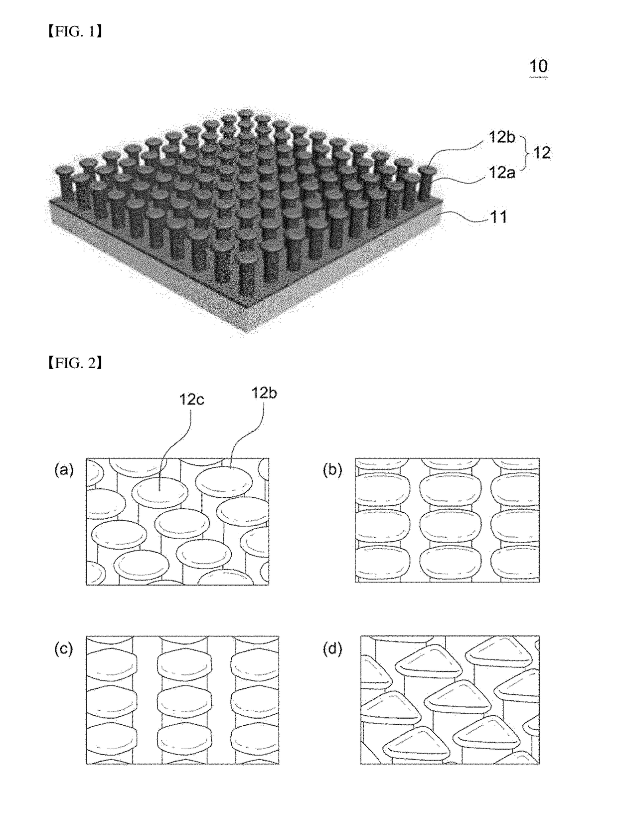
[0059]FIG. 1 is a perspective view of a transfer assembly for transferring LED structures according to the present invention, FIG. 2 shows exemplary views of shapes of adsorption units of a transfer assembly for transferring LED structures according to the present invention, FIG. 3 is an exemplary view of a ciliary unit of a transfer assembly for transferring LED structures according to the present invention, and FIGS. 4 to 8 are cross-sectional views showing a fabrication process of a transfer assembly for transferring LED structures according to the present invention.

[0060]As shown in FIGS. 1 to 3, a transfer assembly 10 according to the present invention includes a body unit 11 and ciliary units 12 so that adhesive members, that is, the ciliary units 12, arranged in an arbitrary pattern on the body unit 11 may have van der Waals attractive force or capillary attractive force by coming into contact with LED structures, which are transfer t...

example 2

FABRICATION EXAMPLE 2 OF TRANSFER ASSEMBLY

[0086]FIG. 9 is a cross-sectional view of another transfer assembly according to the present invention.

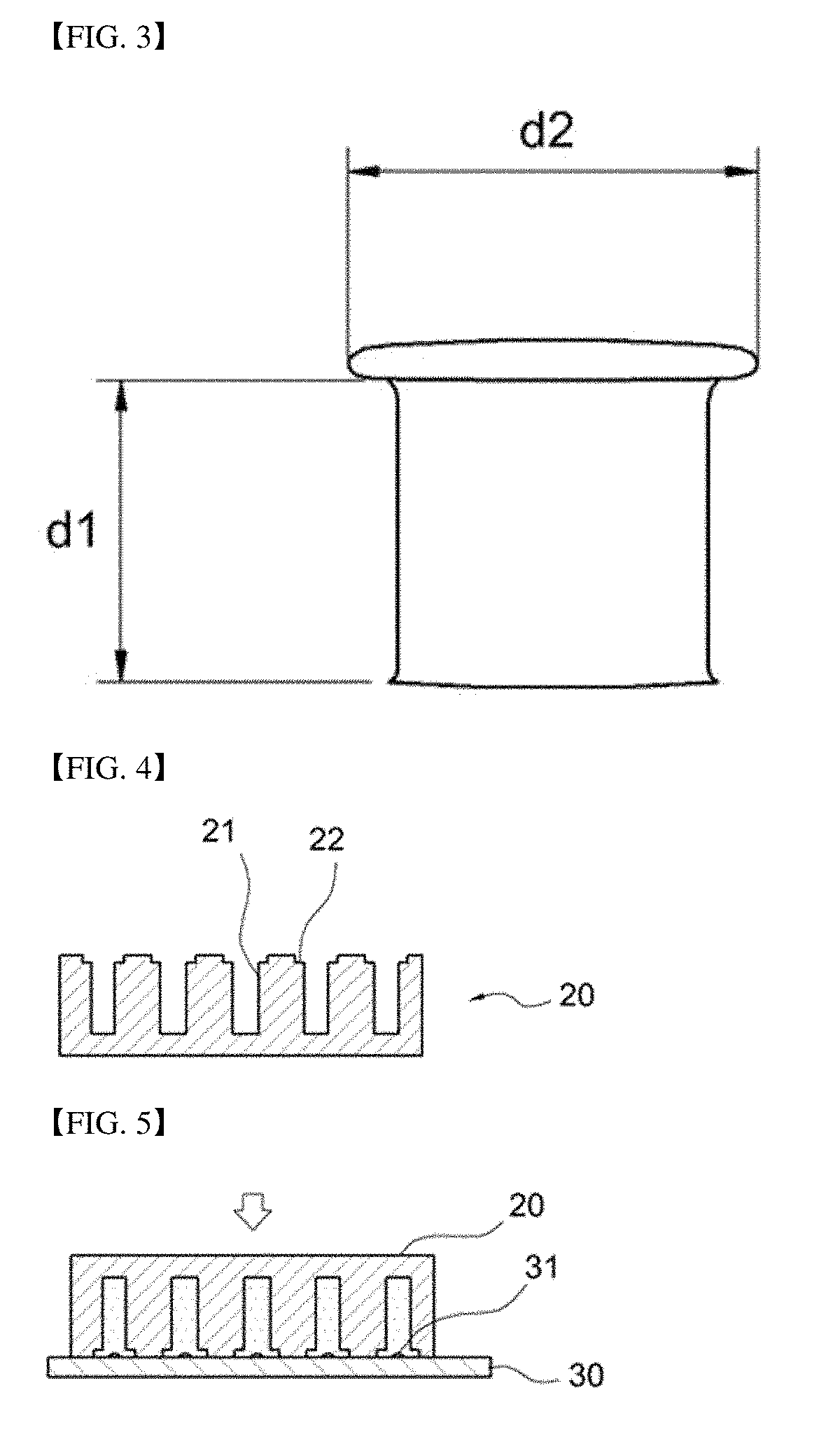
[0087]Referring to FIG. 9, a transfer assembly 10a includes a body unit 11a in the form of a flat board and an adhesive unit 11c which is applied to the body unit 11a and comes in contact with a surface of the LED structures 100 to provide adhesive strength. Preferably, the transfer assembly 10a is made of a polymer resin.

[0088]Also, a plurality of protrusion units 11b protrude from an upper surface of the body unit 11a by a predetermined length to form an arbitrary pattern such that the transfer assembly 10a may easily come into contact with the LED structures 100.

[0089]The protrusion units 11b have a height P1 of 0 μm to 50 μm and a pitch P2 of 1 μm to 300 μm, and the height P1 of 0 μm denotes that the protrusion units 11b are not installed.

[0090]In other words, the adhesive strength of the transfer assembly 10a according to FIG. 9 is onl...

first embodiment

[0091]FIGS. 10 to 23 are cross-sectional views, perspective views, and a block diagram illustrating a process of transferring LED structures according to the first embodiment of the present invention.

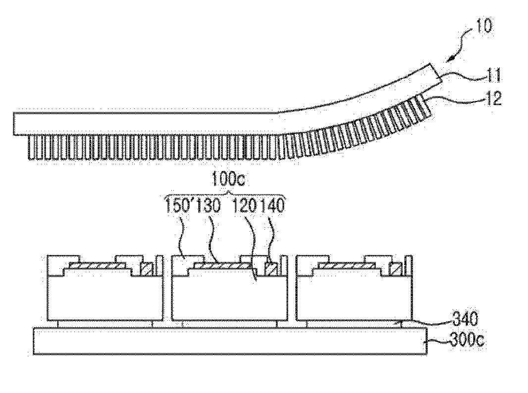
[0092]Referring to FIG. 10, an epitaxial structure 120 is formed on a growth substrate 110, and second electrodes 130 are formed on the epitaxial structure 120.

[0093]A sapphire substrate, a silicon substrate, or the like may be used as the growth substrate 110, and substrates made of various materials may be used as long as they have an epitaxial structure for crystal growth.

[0094]The epitaxial structure 120 is formed on the growth substrate 110 and has a first semiconductor layer 121, an active layer 122, and a second semiconductor layer 123. A buffer layer may be formed between the growth substrate 110 and the first semiconductor layer 121.

[0095]The first semiconductor layer 121 may be an n-type nitride semiconductor layer, the second semiconductor layer 123 may be a p-type nitride se...


PUM


Abstract

The present invention is intended to provide a light-emitting diode (LED) structure which can be easily transferred onto another substrate, a transfer assembly whose adhesive strength with LED structures can be maintained in spite of repetitive transfer processes, LED structures and a transfer assembly for selectively transferring the LED structures, and a transfer method using the same.

Description

CROSS-REFERENCE TO RELATED APPLICATION[0001]This application is Continuation In Part (CIP) of PCT / KR2016 / 014262, filed Dec. 7, 2016, which claims priority to Korean Patent Application No. 10-2016-0034445 filed on Mar. 22, 2016 and all the benefits accruing therefrom under 35 U.S.C. § 119, the contents of which are incorporated by reference in their entirety.TECHNICAL FIELD[0002]The present invention relates to a light-emitting diode (LED) structure, a transfer assembly, and a transfer method using the same, and more particularly, to an LED structure which can be easily transferred onto another substrate, a transfer assembly whose adhesive strength with LED structures can be maintained in spite of repetitive transfer processes, LED structures and a transfer assembly for selectively transferring the LED structures, and a transfer method using the same.BACKGROUND ART[0003]Recently, the demand for lighting fixtures and the like composed of a light-emitting diode (LED) is explosively inc...

Claims


Application Information

Patent Timeline
Patent Type & Authority Applications(United States)
IPC IPC(8): H01L33/00H01L25/075H01L33/62H01L21/66H01L33/32H01L33/06
CPCH01L33/0079H01L25/0753H01L33/62H01L22/20H01L33/007H01L33/32H01L33/06H01L33/36H01L33/44H01L2933/0066H01L2933/0016H01L2933/0025H01L33/0093H01L33/0095H01L33/00H01L33/005H01L2924/12041
Inventor JEUNG, TAKCHOI, WON-SIKPARK, JUN-BEOMBAEK, JONG-HYEOB
Owner KOREA PHOTONICS TECH INST
Why Eureka
Try Eureka