
Memory systems having extended product lifetime and methods of operating the same

a memory system and product life technology, applied in error detection/correction, redundant data error correction, instruments, etc., can solve the problems of poor write endurance of nonvolatile memory devices such as pram devices or rram devices, and relatively high error rate of nonvolatile memory devices

Active Publication Date: 2018-08-09
SK HYNIX INC
View PDF5 Cites 12 Cited by
  • Summary
  • Abstract
  • Description
  • Claims
  • Application Information

AI Technical Summary

Benefits of technology

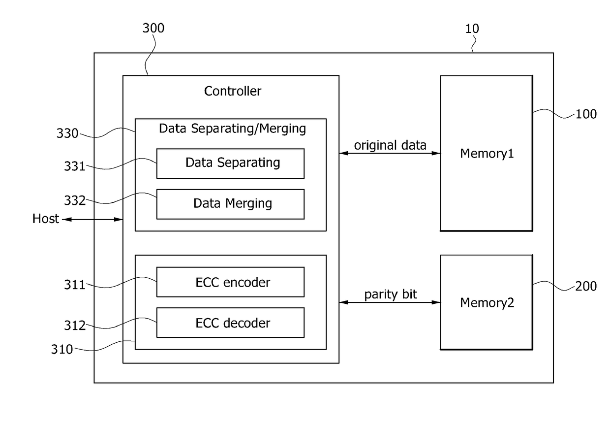
This patent is about memory systems that have a longer lifespan and methods of operating them. The technical effect of this patent is to provide a memory system that can use two memory devices with different write endurances. The controller performs error correction and data inversion processes to generate a binary data stream that includes original data, parity data, and metadata. The metadata includes information on whether the code is inverted. The separated original data and metadata are written into the first and second memory devices, respectively, to ensure that the original data is always written to the first memory device with higher write endurance. This allows for more data to be stored and reduces the risk of data loss in case of power failures or other events that may cause damage to the memory devices.

Problems solved by technology

Although NAND-type flash memory devices are widely used as a nonvolatile memory device, the NAND-type flash memory devices may have some disadvantages in that a read operation and a write operation are achieved in units of pages and an erasure operation is performed in units of blocks.
However, the nonvolatile memory devices may generally exhibit a poor write endurance (corresponding to the maximum number of times that a datum can be repeatedly written into the same memory cell without error), as compared with volatile memory devices.
Thus, the nonvolatile memory devices such as the PRAM devices or the RRAM devices may exhibit a relatively high error rate as compared with the NAND-type flash memory devices, even though a single level cell (SLC) structure is employed in the nonvolatile memory devices.

Method used


Image

  • Memory systems having extended product lifetime and methods of operating the same
  • Memory systems having extended product lifetime and methods of operating the same
  • Memory systems having extended product lifetime and methods of operating the same

Examples


Embodiment Construction

[0027]In the following description of the embodiments, it will be understood that the terms “first” and “second” are intended to identify an element, but not used to define only the element itself or to mean a particular sequence. In addition, when an element is referred to as being located “on”, “over”, “above”, “under”, or “beneath” another element, it is intended to mean relative position relationship, but not used to limit certain cases that the element directly contacts the other element, or at least one intervening element is present therebetween. Accordingly, the terms such as “on”, “over”, “above”, “under”, “beneath”, “below”, and the like that are used herein are for the purpose of describing particular embodiments only and are not intended to limit the scope of the present disclosure. Further, when an element is referred to as being “connected” or “coupled” to another element, the element may be electrically or mechanically connected or coupled to the other element directl...


PUM


Abstract

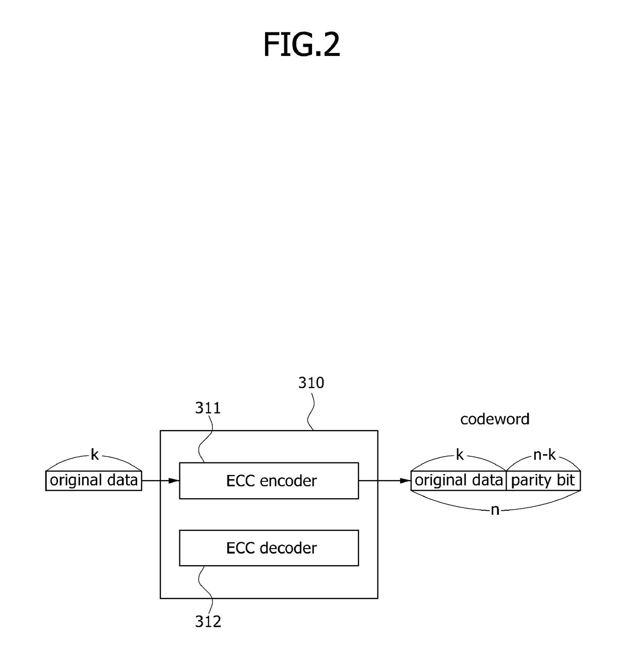
A memory system includes a first memory device, a second memory device, and a controller. The second memory device has a write endurance which is higher than a write endurance of the first memory device. The controller performs an error correction process on original data outputted from a host to generate a codeword including the original data and parity data. The controller separates the codeword into the original data and the parity data to write the separated original data into the first memory device and to write the separated parity data into the second memory device.

Description

CROSS-REFERENCE TO RELATED APPLICATIONS[0001]The present application claims priority under 35 U.S.C 119(a) to Korean Application No. 10-2017-0016451, filed on Feb. 6, 2017, which is herein incorporated by reference in its entirety.BACKGROUND1. Technical Field[0002]Various embodiments of the present disclosure generally relate to memory systems and methods of operating the same and, more particularly, to memory systems having extended product lifetime and methods of operating the memory systems.2. Related Art[0003]Nonvolatile memory (NVM) devices such as ferroelectric random access memory (FRAM) devices, magnetic RAM (MRAM) devices, phase change RAM (PRAM) devices, or the like are very attractive as the next generation of memory devices. This is because the FRAM devices, the MRAM device, the PRAM devices or the like may exhibit a low power consumption characteristic and may access their memory cells in units of bytes with nonvolatile memory characteristics. Although NAND-type flash m...

Claims


Application Information

Patent Timeline
IPC IPC(8): G06F11/10G11C29/52
CPCG06F11/1068G11C29/52G11C29/04G11C29/42G11C2029/0411G06F11/1048G06F3/0649G06F11/10G06F3/0658G06F3/0659G06F3/0685G06F11/108
Inventor BAEK, JINHOPARK, ILSONG, DA EUNLEE, HOKYOONJOO, YOUNGPYO
Owner SK HYNIX INC
Learn More