

Approach to bottom dielectric isolation for vertical transport fin field effect transistors
a technology of vertical transport fin and dielectric isolation, which is applied in the direction of basic electric elements, electrical equipment, semiconductor devices, etc., can solve the problems of difficult formation of individual components and electrical contacts
- Summary
- Abstract
- Description
- Claims
- Application Information
AI Technical Summary
Benefits of technology
Problems solved by technology
Method used
Image

Examples
Embodiment Construction
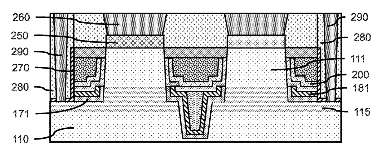
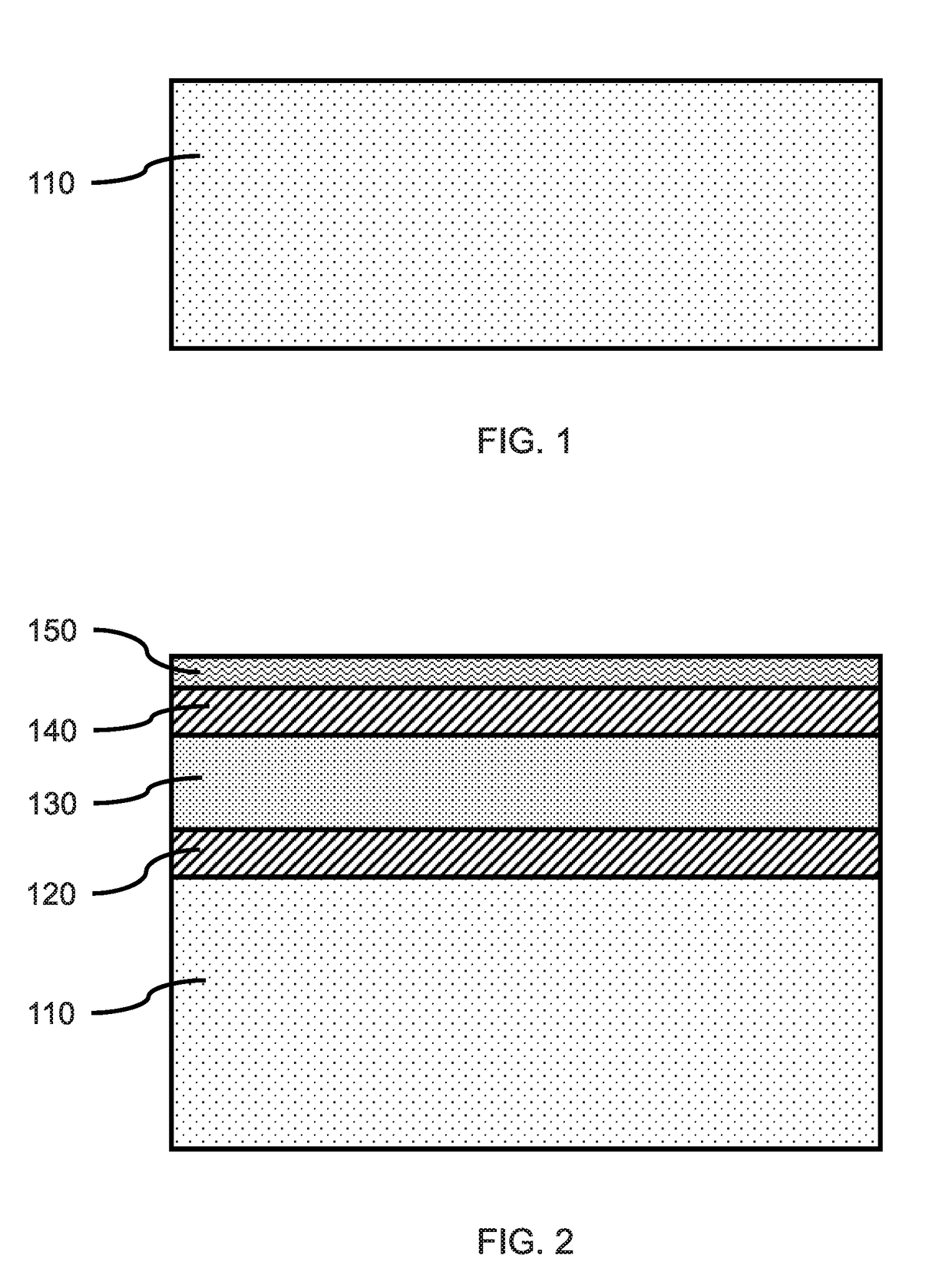
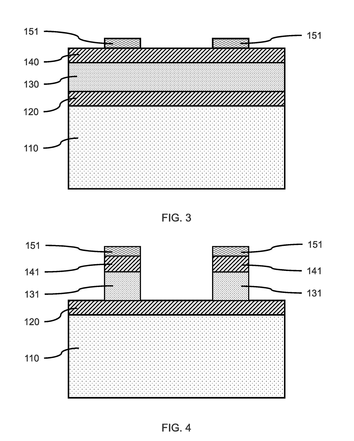
[0036]Principles and embodiments of the present invention relate generally to forming bottom spacers having a more uniform thickness between vertical fins that may vary in pitch and fin pattern density. The bottom spacer can include two layers formed in a manner that does not vary with the distance between adjacent vertical fins. In various embodiments, an oxide liner layer and a nitride spacer layer can be formed on a substrate and vertical fin(s) by thermal atomic layer deposition (Thermal ALD) or plasma enhanced atomic layer deposition (PEALD) to provide a bottom spacer for a vertical transport field effect transistor (VTFET), where the current flows through the FinFET perpendicularly to the plane of the substrate.
[0037]Principles and embodiments of the present invention also relates generally to a U-shaped or L-shaped spacer trough that is conformally deposited on the substrate and vertical fins to have a predetermined thickness that is insensitive to trench width (i.e., inter-f...
PUM
 Abstract
Description
Claims
Application Information