

Prober
a technology of prober and electrode pads, applied in the field of prober, can solve the problems of difficulty in enhancing the reliability of electrical contact between the electrode pads on the wafer and the probe, and achieve the effects of enhancing the reliability of electrical contact, and enhancing the reliability of conta
- Summary
- Abstract
- Description
- Claims
- Application Information
AI Technical Summary
Benefits of technology
Problems solved by technology
Method used
Image

Examples
first embodiment
[0043]To begin, a first embodiment will be described.
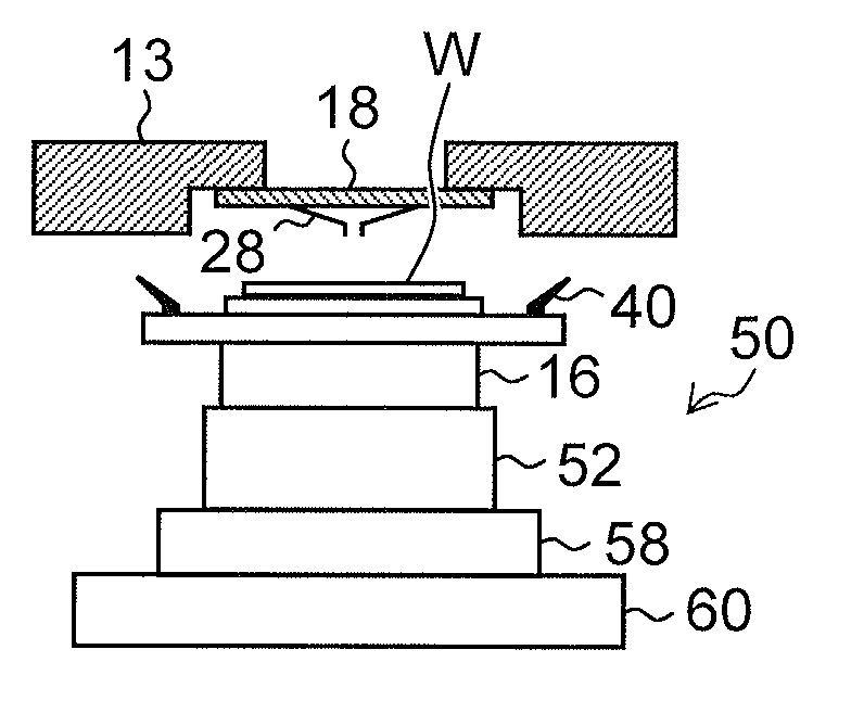
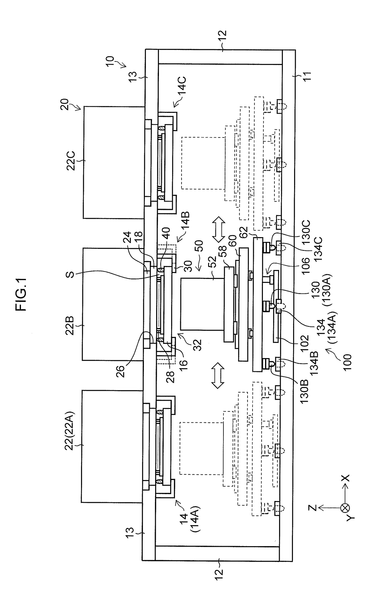
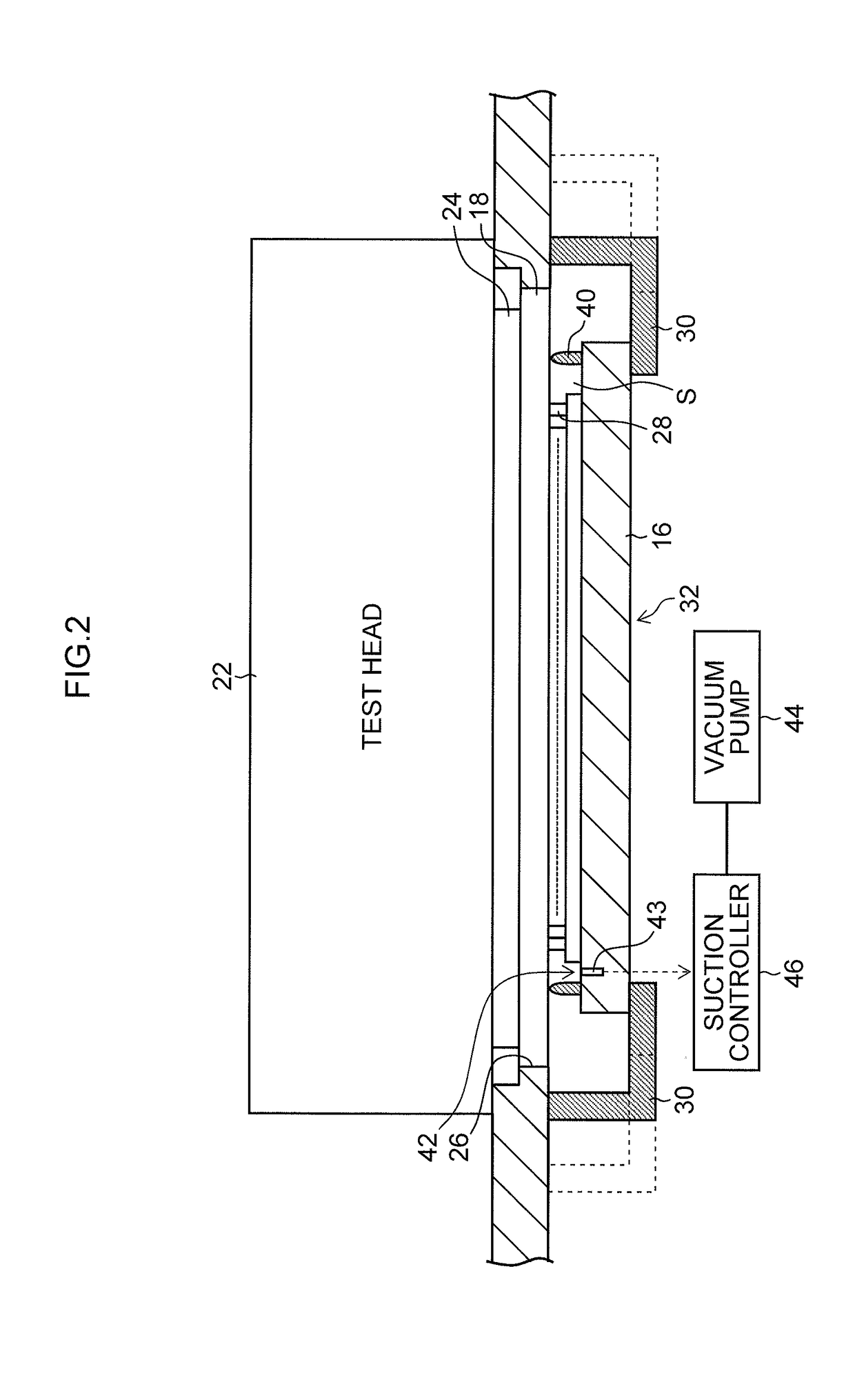
[0044]FIG. 1 is a diagram illustrating a schematic configuration of a system that performs wafer level inspection according to the first embodiment. The system that performs the wafer level inspection includes: a prober 10 that brings metal electrode pads of each chip on a wafer (hereinafter, also referred to as electrode pads on a wafer) into contact with probes; and a tester 20 that is electrically connected to the probes, supplies power and a test signal for electrical inspection to each chip, and detects an output signal from each chip to measure whether the proves normally operate.
[0045]In FIG. 1, a base 11, side plates 12, and a head stage 13 configure a housing of the prober 10. In some cases, an upper plate supported by the side plates 12 is provided, and the head stage 13 is provided on the upper plate.
[0046]The prober 10 is provided with a plurality of measuring units (first to third measuring units) 14A to 14C. The meas...
second embodiment
[0119]Now, a second embodiment will be described. Hereinafter, description of parts that are common with the above embodiments will be omitted, and characteristic parts of this embodiment will be mainly described.
[0120]FIGS. 11A to 11C are diagrams illustrating an example of inspection operation including a probe contact method using a prober 10 according to the second embodiment.
[0121]In the second embodiment, a wafer chuck has a different configuration from the wafer chuck 16 according to the above first embodiment. That is, a wafer chuck 16A according to the second embodiment is equivalent to a wafer chuck obtained by providing the wafer chuck 16 illustrated in FIG. 10A to FIG. 10E with a communication hole 16Aa (an example of a communication path) that communicates the internal space S to external environment and is opened and closed by shutter unit (shutter) 48. The communication hole 16Aa is provided inside the wafer chuck 16A, and passes through a region near outer periphery ...
third embodiment
[0132]Now, a third embodiment will be described. Hereinafter, description of parts that are common with the above embodiments will be omitted, and characteristic parts of this embodiment will be mainly described.
[0133]In the first embodiment, after the final contact step (for example, the second contact) is performed, the depressurizing step of depressurizing the sealed internal space S surrounded by the wafer chuck 16, the probe card 18 and the ring-shaped seal member 40 is performed to draw the wafer chuck 16 toward the probe card 18. At this time, movement of the wafer chuck 16 in the horizontal direction (X and Y directions) is regulated only by contact pressure between the electrode pads on the wafer W and the probes 28 (that is, stylus pressure of the probe card 18). Therefore, when disturbance such as vibration is received from the outside at the time of performing the depressurizing step, horizontal positional deviation or inclination is likely to occur in the wafer chuck 16...
PUM
 Abstract
Description
Claims
Application Information