
Imaging device and solid-state imaging element used in same

a solid-state imaging and imaging device technology, applied in the direction of distance measurement, instruments, surveying and navigation, etc., can solve the problem of speeding up that is not possible, and achieve the effect of eliminating aliasing in distance measurement and high distance measurement accuracy

Inactive Publication Date: 2018-09-13
PANASONIC INTELLECTUAL PROPERTY MANAGEMENT CO LTD
View PDF8 Cites 18 Cited by
  • Summary
  • Abstract
  • Description
  • Claims
  • Application Information

AI Technical Summary

Benefits of technology

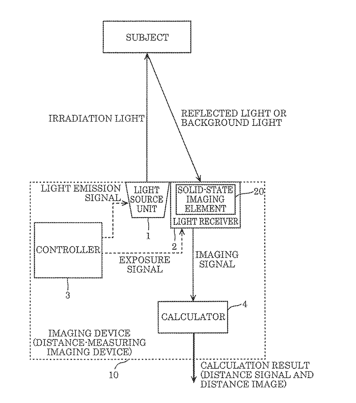
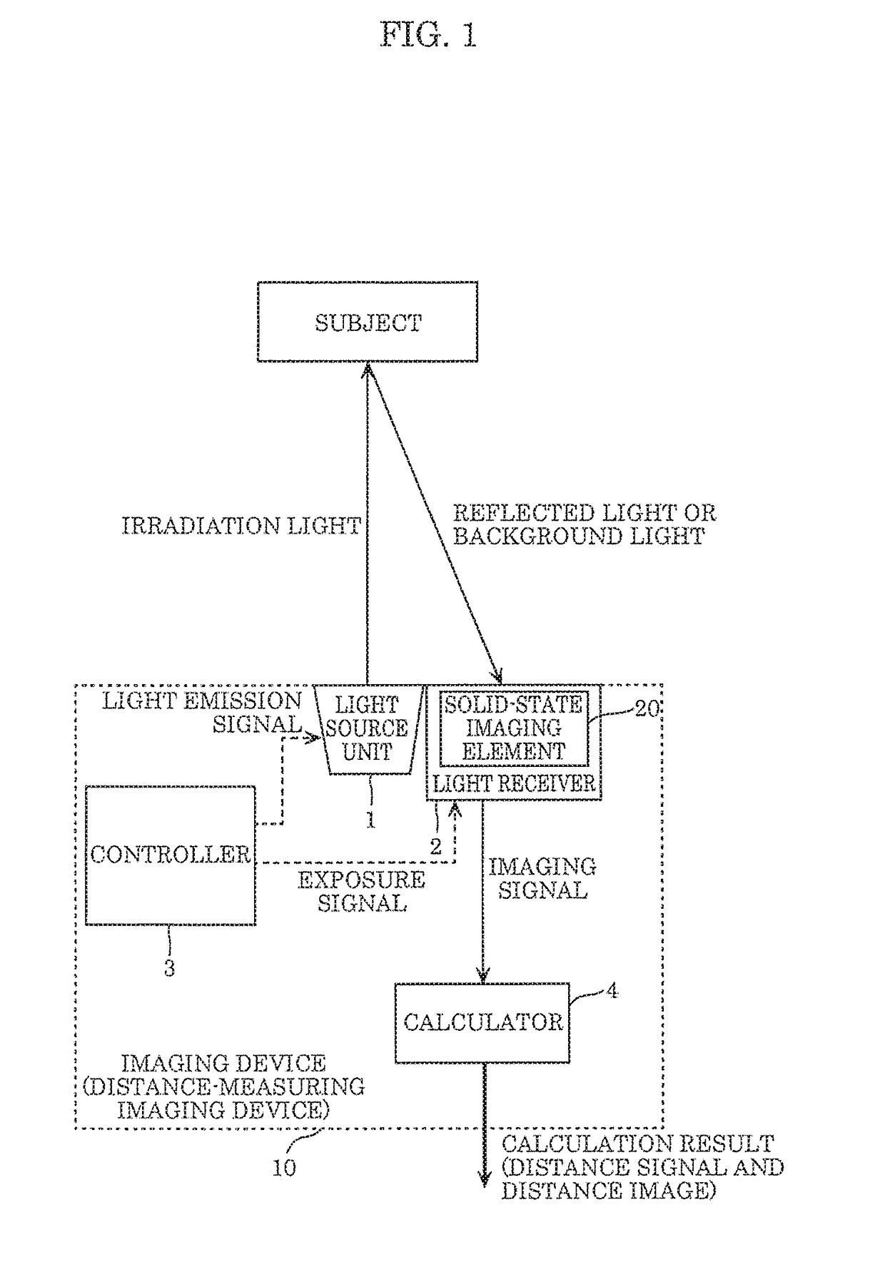
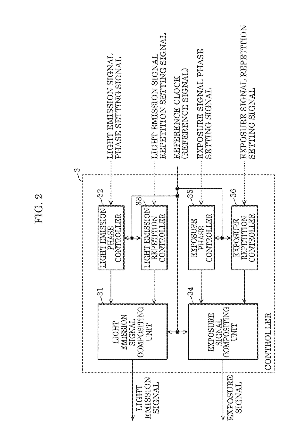
The present invention aims to provide an imaging device that can accurately measure distance without losing accuracy or creating "aliasing" in the distance measurement. The device uses a controller that causes the signals detected by the same pixel to be accumulated through multiple light emissions and exposures, and to differentiate the timing of the light emission and exposure. The invention achieves high distance measurement accuracy and removal of "aliasing" in distance measurement without slowing down the frame rate.

Problems solved by technology

Accordingly, the above-mentioned conventional technique is problematic in that the frame rate is limited by low modulation frequencies and thus, speeding up is not possible.

Method used


Image

  • Imaging device and solid-state imaging element used in same
  • Imaging device and solid-state imaging element used in same
  • Imaging device and solid-state imaging element used in same

Examples


embodiment 1

Variation 2 of Embodiment 1

[0106]FIG. 10 illustrates the sequence of signal processing in an imaging device according to Variation 2 of Embodiment 1. Similar to Embodiment 1, S0, S1, and S2 light emission / exposure signals have different cycles (duties), and furthermore, non-light emission periods are established so as to make at least the average cycles for light emission the same.

[0107]With this, the S0 light emission signal and the S2 light emission signal have the same heat quantity per unit time; thus, in particular, it is possible to reduce variations in the performance and characteristics of distance measurement by preventing the effects of the thermal characteristics of the light source unit (the light source (such as the light-emitting element, the LED, and the LD)) and the drive circuit (driver) for the light source which significantly affect the characteristics of the imaging device.

[0108]Thus, in Variation 2 of the present embodiment, in addition to the same advantageous ...

embodiment 2

Variation 2 of Embodiment 2

[0126]FIG. 13 illustrates an example of the timings for the light emission signal and the exposure signal and the exposure amount of imaging device 10 according to Variation 2 of the present embodiment.

[0127]The present embodiment provides, as described above, a plurality of signal accumulators (as an example, three signal accumulators) in which signals (accumulation signals) detected by the same pixel included in solid-state imaging element 20 are accumulated. The length of each of the first, second, and third exposure signal periods in the first, second, and third light emission / exposure periods in which the signals are accumulated in the plurality of signal accumulators is set to To which is the same as the length of the light emission signal period. The delay time of the first exposure signal with respect to the timing at which light source unit 1 receives the light emission signal and emits light is set to 0.

[0128]Thus, the first exposure signal perio...


PUM


Abstract

An imaging device includes: a controller which generates a light emission signal and an exposure signal; a light source unit which receives the light emission signal and emits light; a light receiver which obtains the exposure amount of reflected light at a timing in accordance with the exposure signal; and a calculator which outputs a distance signal (distance image) by calculation on the basis of the amount of signals included in imaging signals received from the light receiver. The controller generates two or more patterns of varying phase relationships between the light emission signal and the exposure signal, and outputs the light emission signal and the exposure signal in a cycle that is different between at least two of the patterns.

Description

CROSS REFERENCE TO RELATED APPLICATIONS[0001]This application is a U.S. continuation application of PCT International Patent Application Number PCT / JP2016 / 004837 filed on Nov. 9, 2016, claiming the benefit of priority of U.S. Provisional Application No. 62 / 255,645 filed on Nov. 16, 2015, the entire contents of which are hereby incorporated by reference.BACKGROUND1. Technical Field[0002]The present disclosure relates to an imaging device and a solid-state imaging element used in the imaging device.2. Description of the Related Art[0003]Among methods for sensing an object or measuring a distance, the time-of-flight (TOF) method is known in which a distance is measured using flight time that light takes to travel to and return from a measurement object.[0004]Unexamined Patent Application Publication (Translation of PCT Application) No. 2013-538342 discloses de-aliasing for disambiguating time of round-trip of detected light during repeated light emission and exposure without degradatio...

Claims


Application Information

Patent Timeline
Patent Type & Authority Applications(United States)
IPC IPC(8): G01S17/89G01C3/08G01S17/10G01S7/487G01S7/48G01S7/486G01S7/4865G01S17/894
CPCG01S17/89G01C3/08G01S17/10G01S7/487G01S7/4808G01S7/4865G01S7/4868G01S17/894
Inventor TAKANO, HARUKAKANEMITSU, TOMOHIKOHASUKA, TSUYOSHIOTANI, MITSUHIKO
Owner PANASONIC INTELLECTUAL PROPERTY MANAGEMENT CO LTD
Learn More