

Fin-type field effect transistors (finfets) with replacement metal gates and methods
- Summary
- Abstract
- Description
- Claims
- Application Information
AI Technical Summary
Benefits of technology
Problems solved by technology
Method used
Image

Examples
first embodiment
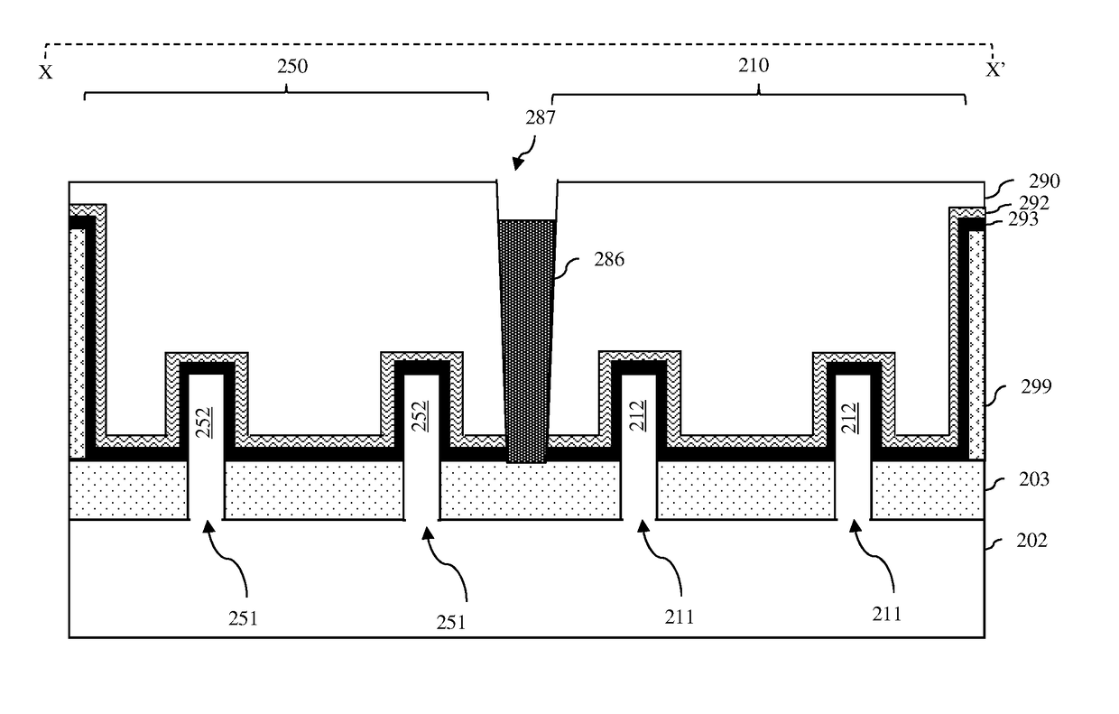
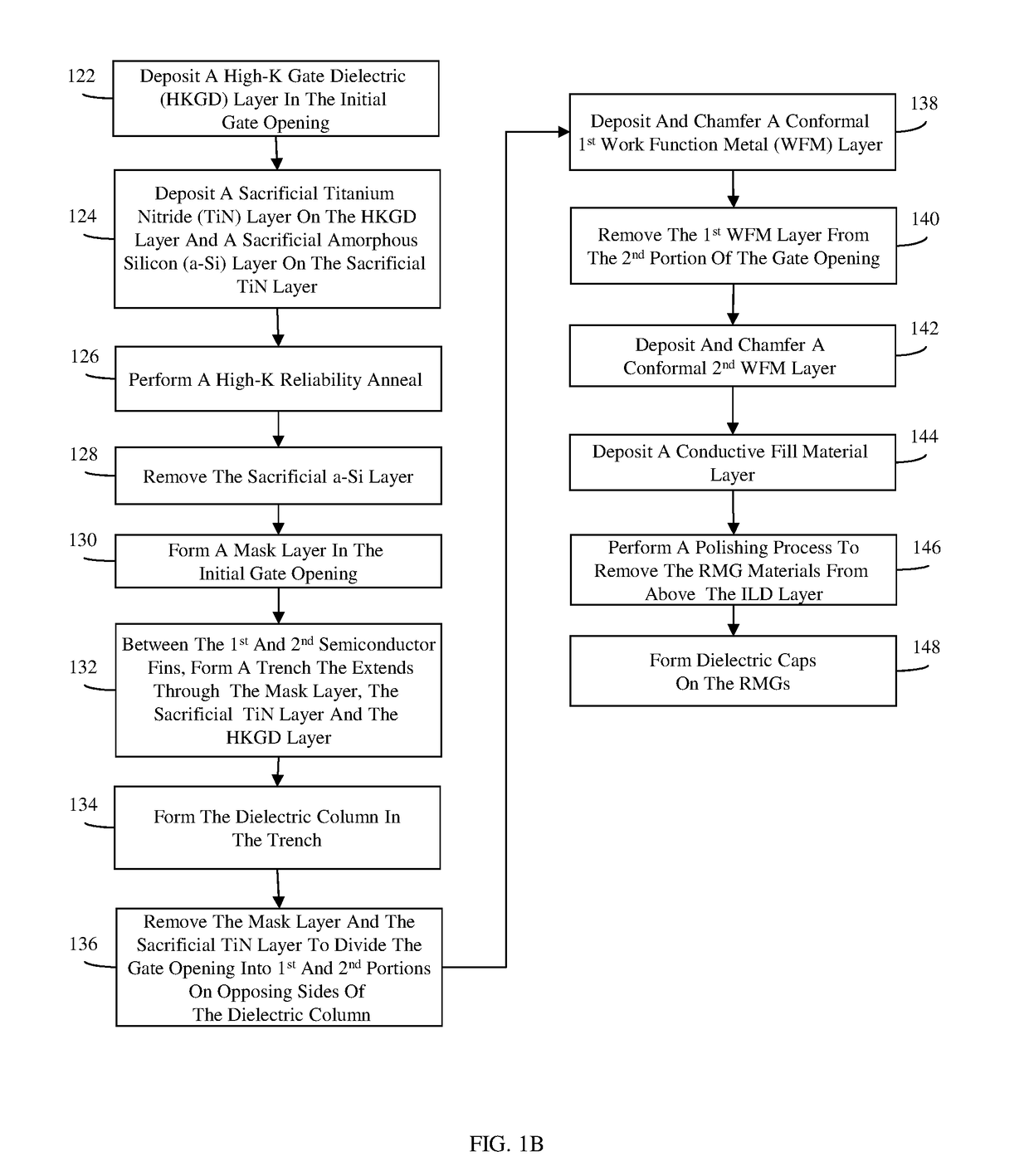
[0054]More specifically, referring to FIG. 1B, in the method, a gate dielectric layer and, particularly, a high-K gate dielectric layer 293 can be conformally deposited in the gate opening 294 (122). An anneal process can subsequently be performed to improve the reliability of the high-K gate dielectric layer 293. For example, a conformal sacrificial titanium nitride layer 292 can be deposited on the high-K gate dielectric layer 293 and a sacrificial amorphous silicon layer 291 can be deposited onto the sacrificial titanium nitride layer 292 (124). In one exemplary embodiment, the fin pitch can be approximately 15-25 nm (e.g., 20 nm), the thickness of the high-K gate dielectric layer 293 can be approximately 1-2 nm (e.g., 1.5 nm), the thickness of the sacrificial titanium nitride layer 292 can be approximately 1-2 nm (e.g., 1.5 nm) and the thickness of the sacrificial amorphous silicon layer 291 can be approximate 3-5 nm (e.g., 4 nm). The partially completed structure can then be su...
second embodiment
[0063]Alternatively, referring to FIG. 1C, in the method, a gate dielectric layer and, particularly, a high-K gate dielectric layer 293 can be conformally deposited in the gate opening 294 (150, see FIGS. 18A-18B). An anneal process can subsequently be performed to improve the reliability of the high-K gate dielectric layer 293. For example, a conformal sacrificial titanium nitride layer can be deposited on the high-K gate dielectric layer 293 and a sacrificial amorphous silicon layer can be deposited onto the sacrificial titanium nitride layer (152). In one exemplary embodiment, the fin pitch can be approximately 15-25 nm (e.g., 20 nm), the thickness of the high-K gate dielectric layer 293 can be approximately 1-2 nm (e.g., 1.5 nm), the thickness of the sacrificial titanium nitride layer 292 can be approximately 1-2 nm (e.g., 1.5 nm) and the thickness of the sacrificial amorphous silicon layer 291 can be approximate 3-5 nm (e.g., 4 nm). The partially completed structure can then be...
PUM
 Abstract
Description
Claims
Application Information