

Display panel and method of producing display panel
a technology of display panel and assembly method, which is applied in the direction of instruments, non-linear optics, optics, etc., can solve the problems that the sealing member may not be able to withstand the force, and achieve the effect of reducing the frame siz
- Summary
- Abstract
- Description
- Claims
- Application Information
AI Technical Summary
Benefits of technology
Problems solved by technology
Method used
Image

Examples
first embodiment
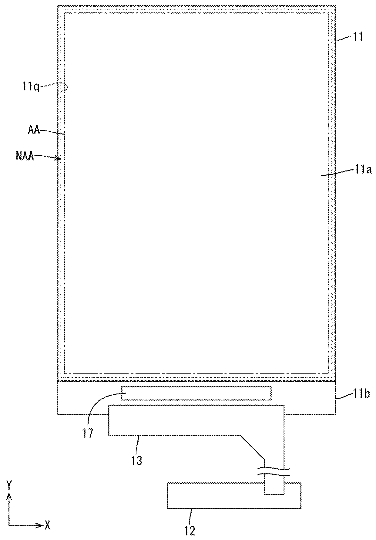
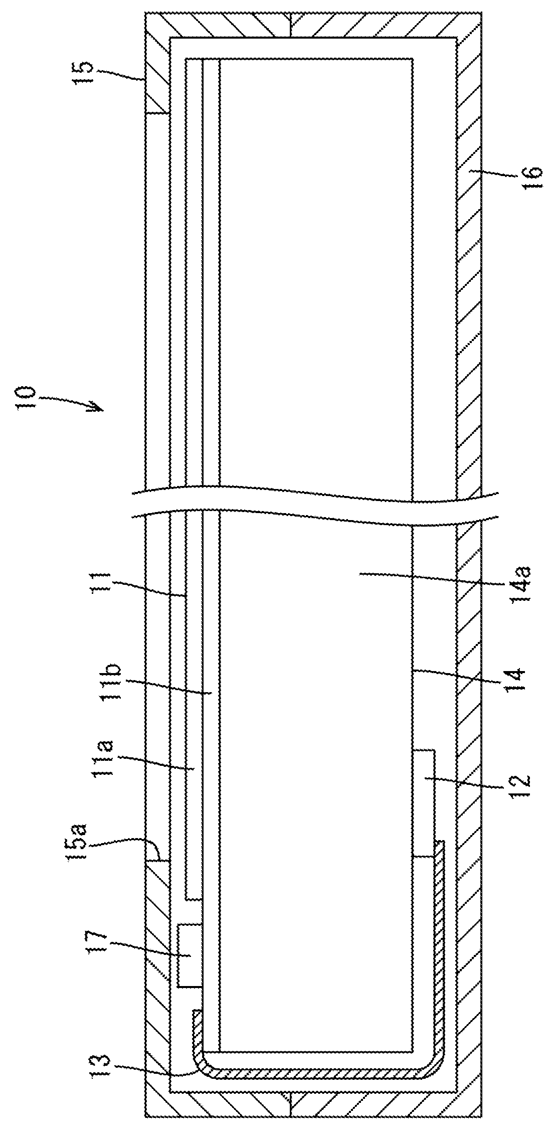
[0054]A first embodiment of the present invention will be described with reference to FIGS. 1 to 20. In this section, a liquid crystal display device 10 will be described. X-axes, Y-axes, and Z-axes may be present in drawings. The axes in each drawing correspond to the respective axes in other drawings to indicate the respective directions. A vertical direction of the liquid crystal display device 10 is defined based on FIGS. 2 to 4. Upper sides and lower sides in in FIGS. 2 to 4 correspond to a front side and a rear side of the liquid crystal display device 10, respectively.
[0055]As illustrated in FIGS. 1 and 2, the liquid crystal display device 10 includes a liquid crystal panel 11 (a display panel), a driver 17 (a panel driver), a control circuit board 12 (an external signal source), a flexible circuit board 13 (an external connecting component), and a backlight unit 14 (a lighting device). The liquid crystal panel 11 is configured to display images. The liquid crystal panel 11 i...
second embodiment
[0094]A second embodiment of the present invention will be described with reference to FIGS. 21 and 22. The second embodiment includes a light blocking portion without a frame section. Configurations, functions, and effects similar to those of the first embodiment will not be described.
[0095]As illustrated in FIGS. 21 and 22, a liquid crystal panel 111 in this embodiment includes a sealing member 111q that is disposed for about entire width of the non-display area NAA. The light blocking portion, which is not illustrated, does not include the frame section. The sealing member 111q is disposed to separate the pixels PX from one another together with a grid section of the light blocking portion. The pixels PX that are disposed at the outermost among the pixels PX that are arranged in the matrix in the display area AA are separated by the outermost section of the grid section of the light blocking portion and the sealing member 111q that collectively surrounds them. Because the frame s...
third embodiment
[0097]A third embodiment of the present invention will be described with reference to FIG. 23. The third embodiment includes a sealing member forming device 40 used in a sealing member forming process, which is different from the first embodiment. Configurations, functions, and effects similar to those of the first embodiment will not be described.
[0098]As illustrated in FIG. 23, in the sealing member forming process in this embodiment, the fusion deposition type sealing member forming device 40 is used. The sealing member forming device 40 includes at least a stage 41, a head 42, and a controller 43. A CF base board 211aM is placed on the stage 41. The head 42 is disposed opposite the CF base board 211aM on the stage 41. The controller 43 is connected to the head 42 and configured to control the head 42. In comparison to the powder sintering type sealing member forming device 30 in the first embodiment (see FIG. 10), the fusion deposition type sealing member forming device 40 is pr...
PUM
| Property | Measurement | Unit |
|---|---|---|
| size | aaaaa | aaaaa |
| width | aaaaa | aaaaa |
| mean particle diameter | aaaaa | aaaaa |
Abstract
Description
Claims
Application Information