Optical waveguide display assembly, electronic device, and fabricating method thereof

Inactive Publication Date: 2018-10-04
BOE TECH GRP CO LTD
View PDF5 Cites 1 Cited by
  • Summary
  • Abstract
  • Description
  • Claims
  • Application Information

AI Technical Summary

Benefits of technology

The patent text describes a way to improve the display on an optical waveguide display by adjusting the ability of the display to scatter light. By making certain parts of the display closer to the light source, the incident light can be changed to destroy the total reflection condition and improve display uniform performance. This can help to compensate for uneven display caused by light attenuation.

Problems solved by technology

However, the display module of the optical waveguide transparent display device may have poor display uniformity due to the attenuation effect of the optical waveguide transmission structure of the display module.

Method used


Image

  • Optical waveguide display assembly, electronic device, and fabricating method thereof
  • Optical waveguide display assembly, electronic device, and fabricating method thereof
  • Optical waveguide display assembly, electronic device, and fabricating method thereof

Examples


Embodiment Construction

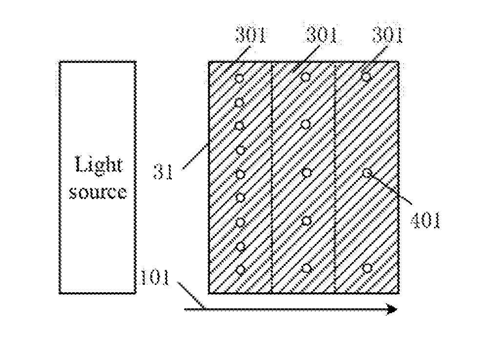
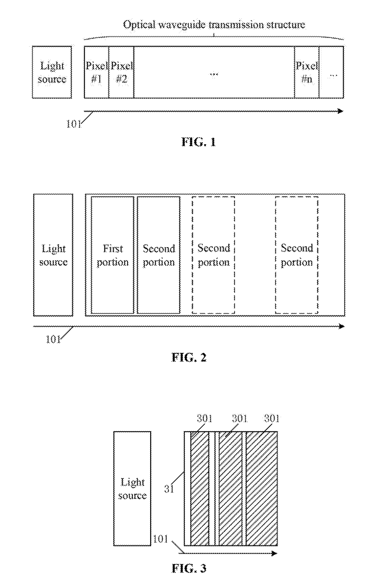
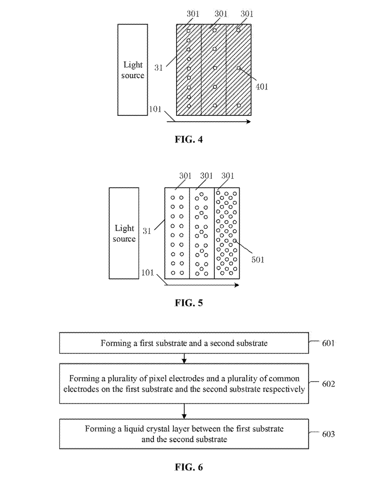
[0032]Reference input now be made in detail to exemplary embodiments of the invention, which are illustrated in the accompanying drawings in order to understand and implement the present disclosure and to realize the technical effect. It should be understood that the following description has been made only by way of example, but not to limit the present disclosure. Various embodiments of the present disclosure and various features in the embodiments that are not conflicted with each other can be combined and rearranged in various ways. Without departing from the spirit and scope of the present disclosure, modifications, equivalents, or improvements to the present disclosure are understandable to those skilled in the art and are intended to be encompassed within the scope of the present disclosure.

[0033]In accordance with various embodiments, the present disclosure provides an optical waveguide display assembly, an electronic device, and a fabricating method thereof.

[0034]In some em...


PUM

PropertyMeasurementUnit
Timeaaaaaaaaaa
Concentrationaaaaaaaaaa
Shapeaaaaaaaaaa

Abstract

An optical waveguide display assembly, an electronic device, and a fabricating method thereof are provided. The optical waveguide display assembly includes: a display region, including a first portion and a second portion with a substantially same area, the first portion being closer to a light source than the second portion; and a macromolecular polymer, in the display region, having a concentration in the first portion lower than that in the second portion, and configured to scatter light emitted from the light source.

Description

CROSS-REFERENCES TO RELATED APPLICATIONS[0001]This application claims the priority of Chinese Patent Application No. 201610618088.2, filed on Jul. 29, 2016, the entire contents of which are incorporated herein by reference.TECHNICAL FIELD[0002]The present disclosure generally relates to the field of display technology, and more particularly, to an optical waveguide display assembly, an electronic device, and a fabricating method thereof.BACKGROUND[0003]As display technology advances, transparent display products have been newly emerged. When a transparent display device is in operation, the user can clearly see scenes behind the transparent display device through the transparent display device. Because of this, the transparent display device has become more popular and has been gradually involved in store windows, smart glasses, smart helmet, and other products.[0004]The transparent display device may include an optical waveguide transparent display module, which may provide higher ...

Claims


Application Information

Patent Timeline
IPC IPC(8): G02F1/1334G02F1/1335G02F1/1343C09K19/54
CPCG02F1/1334G02F1/133524G02F1/133553G02F1/134309C09K19/544G02F2201/123G02F2202/022G02F2201/121C08G63/00G02F1/1333G02F1/133615G02B6/0078G02B6/0061G02B6/00G09F9/00B32B2457/202B32B2457/20C09K2323/03C09K2323/035
Inventor LI, XINCHENG, HONGFEI
Owner BOE TECH GRP CO LTD
Why Eureka
Try Eureka