Image sensor
- Summary
- Abstract
- Description
- Claims
- Application Information
AI Technical Summary
Benefits of technology
Problems solved by technology
Method used
Image

Examples
Embodiment Construction
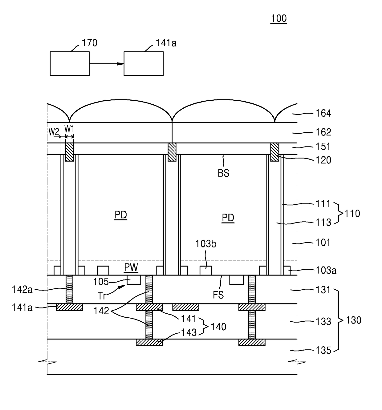
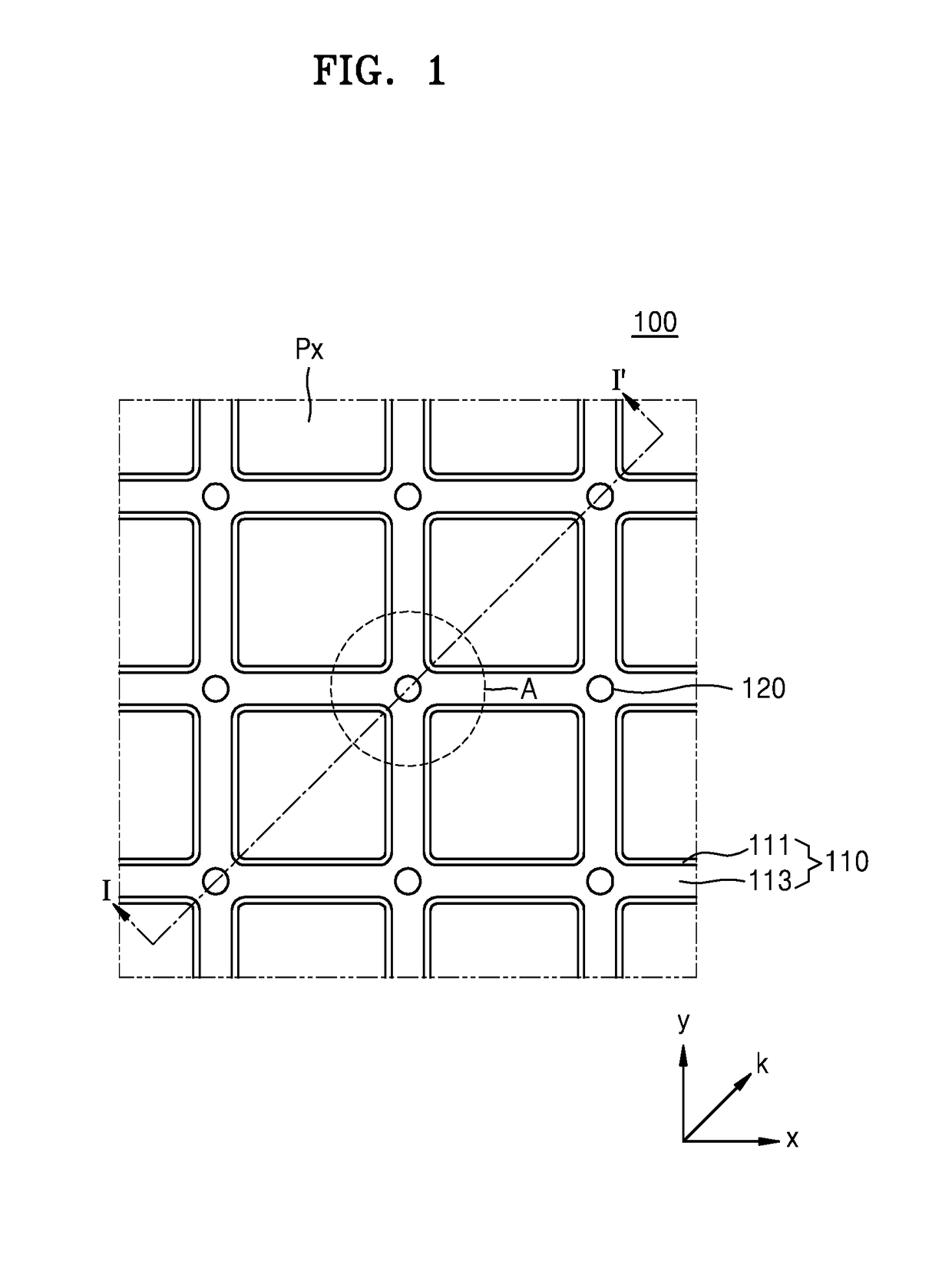
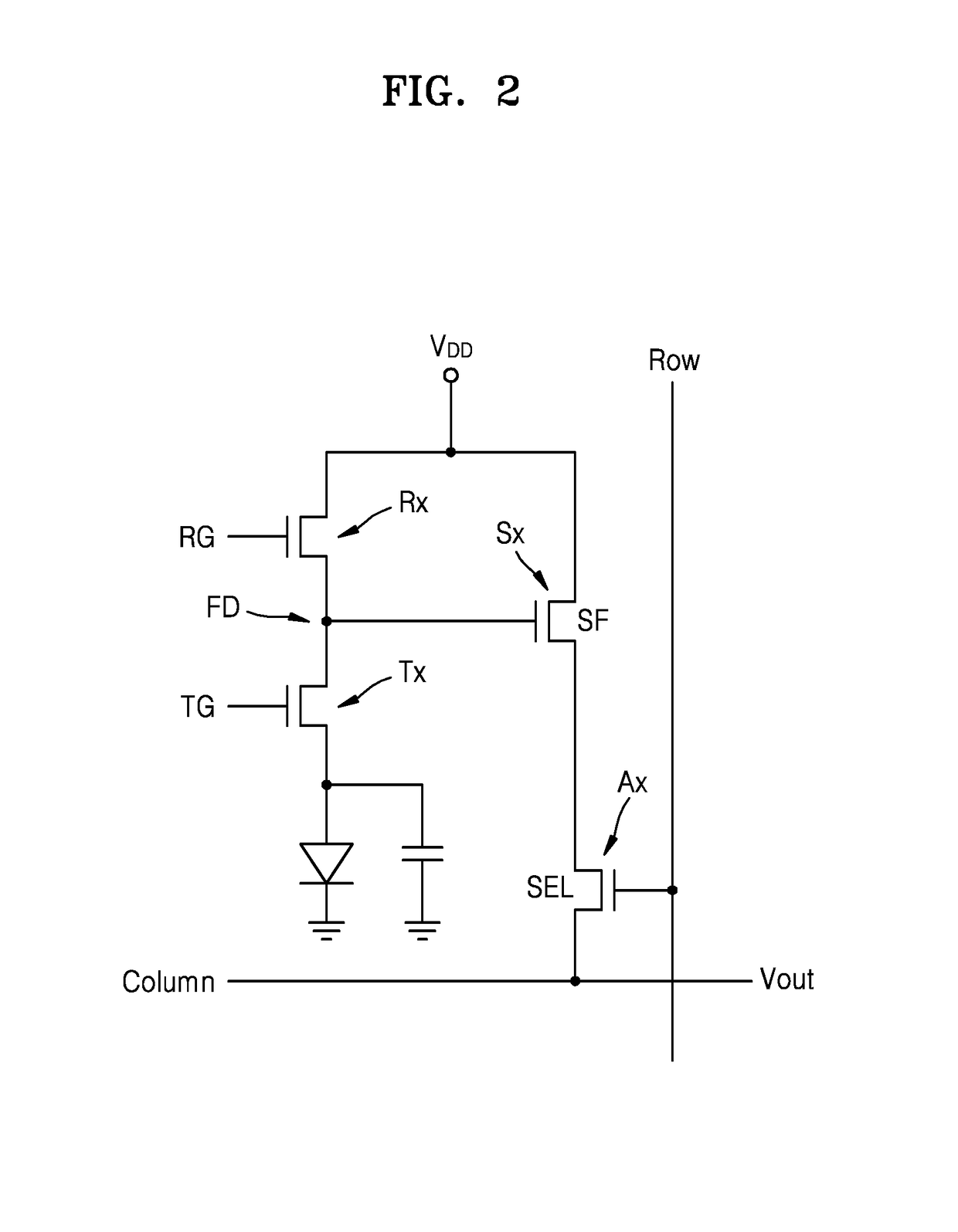
[0018]FIG. 1 is a plan view of a part of a pixel of an image sensor 100 according to an exemplary embodiment and schematically shows only a pixel Px, a pixel separation structure 110, and a back side contact 120 for convenience of understanding. As used herein, singular “a,”“an,” and “the” are intended to cover the plural forms as well, unless the context clearly indicates otherwise. FIG. 2 is a circuit diagram of the pixel Px included in the image sensor 100 of FIG. 1. FIG. 3 is a cross-sectional view taken along line I-I′ of FIG. 1. FIG. 4 is an enlarged view of a portion “A” of the image sensor 100 of FIG. 1.
[0019]Referring to FIGS. 1 through 4, the image sensor 100 includes a substrate 101, a photodiode PD, the pixel separation structure 110, the back side contact 120, a multi-layered interconnection 140, a color filter 162, and a micro-lens 164.
[0020]The substrate 101 may include a silicon bulk wafer or an epitaxial wafer. The epitaxial wafer may include a crystalline layer gro...
PUM
 Abstract
Description
Claims
Application Information
 - Generate Ideas
- Intellectual Property
- Life Sciences
- Materials
- Tech Scout
- Unparalleled Data Quality
- Higher Quality Content
- 60% Fewer Hallucinations
Browse by: Latest US Patents, China's latest patents, Technical Efficacy Thesaurus, Application Domain, Technology Topic, Popular Technical Reports.
© 2025 PatSnap. All rights reserved.Legal|Privacy policy|Modern Slavery Act Transparency Statement|Sitemap|About US| Contact US: help@patsnap.com