Electrode assembly comprising micro-led elements and method for manufacturing same

a micro-led element and assembly technology, applied in the field of electromechanical assembly, can solve the problems of difficult disposed and mounted nano-scale-led elements, unable to be disposed and mounted on a target electrode region with a human hand, and achieve the effect of maximizing light intensity per unit area

Active Publication Date: 2018-10-04
SAMSUNG DISPLAY CO LTD
View PDF4 Cites 19 Cited by
  • Summary
  • Abstract
  • Description
  • Claims
  • Application Information

AI Technical Summary

Benefits of technology

[0007]To address the above described problem, an objective of the present disclosure is to provide an electrode assembly including nano-scale light emitting diode (LED) elements and a method for manufacturing the same, which are capable of maximizing light intensity per unit area by increasing the number of nano-scale-LED elements included in a unit area of the electrode assembly and light extraction efficiency of each of the nano-scale-LED elements, and, at the same time, are capable of connecting the nano-scale-LED elements fabricated in a nanoscale size to an electrode without faults such as an electrical short circuit and the like.
[0030]The electrode assembly of the present disclosure is configured such that a nano-scale light emitting diode (LED) element is three-dimensionally disposed in a space between electrodes so that the number of nano-scale-LED elements included in an electrode line per unit area can be increased, and, at the same time, light extraction efficiency of each of the nano-scale-LED elements can be improved, thereby maximizing light intensity of the electrode assembly per unit area. Also, a space occupied by a single nano-scale-LED element in the electrode assembly can be minimized so that a space in which other nano-scale-LED elements are able to be disposed can be relatively increased such that the number of nano-scale-LED elements included in the electrode assembly can be increased, and thus light intensity can be more increased. Further, a nanoscale nano-scale-LED element is connected to an electrode without faults such as an electrical short circuit and the like so that a defect rate of the electrode assembly can be decreased. Moreover, even though a nano-scale-LED element does not have a specific structural shape to prevent faults such as an electrical short circuit and the like, a detect rate of a nano-scale-LED electrode assembly can be minimized.

Problems solved by technology

Among the above areas of focus, there is still difficulty in the method for mounting a nano-scale-LED element on a disposed electrode, in which it is difficult for the nano-scale-LED element to be disposed and mounted as intended on the disposed electrode according to a limitation in size of the nano-scale-LED element.
This is because the nano-scale-LED element is fabricated at a nanoscale or nano-scalescale size, and thus cannot be disposed and mounted on a target electrode region with a human hand.
In addition, although the nano-scale-LED element is mounted on the target electrode region, it is very difficult to adjust the number of nano-scale-LED elements included in a unit electrode region, a positional relationship between the nano-scale-LED element and the electrode, and the like to match intentions, and the number of LED elements included in a unit area is limited when the nano-scale-LED element is disposed on a two-dimensional plane such that it is difficult to obtain excellent light intensity.
Further, since all nano-scale-LED elements connected to two different electrodes are not able to emit light without faults such as an electrical short circuit and the like, there is a problem in that target light intensity is more difficult to obtain.

Method used


Image

  • Electrode assembly comprising micro-led elements and method for manufacturing same
  • Electrode assembly comprising micro-led elements and method for manufacturing same
  • Electrode assembly comprising micro-led elements and method for manufacturing same

Examples


Embodiment Construction

[0051]Hereinafter, one preferred embodiment of the present disclosure will be described in more detail with reference to the accompanying drawings.

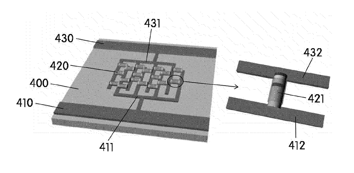
[0052]As is described above, since a nano-scale light emitting diode (LED) element is not disposed and mounted on a target electrode region with a human hand due to a limitation in size of the nano-scale-LED element according to a related art, there is a problem in that it is very difficult for the nano-scale-LED element to be disposed and mounted as intended on an electrode. FIG. 1 is a perspective view of a typical electrode assembly including a nano-scale-LED element, and illustrates a first electrode 310 formed over a base substrate 300, a second electrode 320 formed on the first electrode 310 to be separated therefrom and in parallel therewith, and a nano-scale-LED element 330 connected between the first electrode 310 and the second electrode 320 in a three-dimensionally upright form. In the case of an electrode assembly having such ...


PUM


Abstract

The present invention relates to an electrode assembly comprising nano-scale-LED elements and a method for manufacturing the same and, more specifically, to an electrode assembly comprising nano-scale-LED elements and a method for manufacturing the same, in which the number of nano-scale-LED elements included in a unit area of the electrode assembly is increased, the light extraction efficiency of individual nano-scale-LED elements is increased so as to maximize light intensity per unit area, and at the same time, nano-scale-LED elements on a nanoscale are connected to an electrode without a fault such as an electrical short circuit.

Description

CROSS-REFERENCE TO RELATED APPLICATIONS[0001]This application is a national phase application under 35 U.S.C. § 371 of International Application No. PCT / KR2015 / 012250, filed Nov. 13, 2015, which claims priority to Korean Patent Application No. 10-2014-0161065, filed Nov. 18, 2014, the contents of which applications are incorporated into the present application by reference.TECHNICAL FIELD[0002]The present disclosure relates to an electrode assembly including nano-scale-light emitting diode (LED) elements and a method for manufacturing the same, and more particularly, to an electrode assembly including nano-scale-LED elements and a method for manufacturing the same, which are capable of maximizing light intensity of the electrode assembly per unit area by increasing the number of nano-scale-LED elements included in a unit area of the electrode assembly and light extraction efficiency of each of the nano-scale-LED elements, and, at the same time, are capable of connecting the nano-sca...

Claims


Application Information

Patent Timeline
Patent Type & Authority Applications(United States)
IPC IPC(8): H01L33/08H01L33/06H01L33/24H01L33/32H01L33/38H01L33/44H01L33/00B82B3/00
CPCH01L33/08H01L33/06H01L33/24H01L33/32H01L33/387H01L33/44H01L33/007B82B3/0066H01L2933/0016H01L25/0753H01L33/36H01L33/38
Inventor SUNG, YEON GOOG
Owner SAMSUNG DISPLAY CO LTD
Why Eureka
Try Eureka