
Array substrates and display panels

a display panel and substrate technology, applied in non-linear optics, instruments, optics, etc., can solve the problems of low charging rate of lcds, inability to meet the requirements of high resolution and large dimension, etc., to enhance the charging rate of pixel, enhance the display performance of lcd, and reduce the risk of erroneous charging

Active Publication Date: 2018-10-18
TCL CHINA STAR OPTOELECTRONICS TECH CO LTD
View PDF2 Cites 0 Cited by
  • Summary
  • Abstract
  • Description
  • Claims
  • Application Information

AI Technical Summary

Benefits of technology

The present invention relates to a display panel that improves the charging time of pixels to enhance the charging rate and reduce the risk of incorrect charging. This is achieved by configuring a second transistor within the pixel cell and connecting it to the scanning line, which fixes the pulse width of scanning signals within one scanning period. This extended turn-on period of the first transistor results in an extended charging period for the pixel electrode, leading to improved display performance and reduced risk of erroneous charging.

Problems solved by technology

With the increase of the resolution and the dimension of the LCDs, the charging rate of the LCDs is getting lower, which cannot satisfy the requirement of high resolution and large dimension.

Method used


Image

  • Array substrates and display panels
  • Array substrates and display panels
  • Array substrates and display panels

Examples


first embodiment

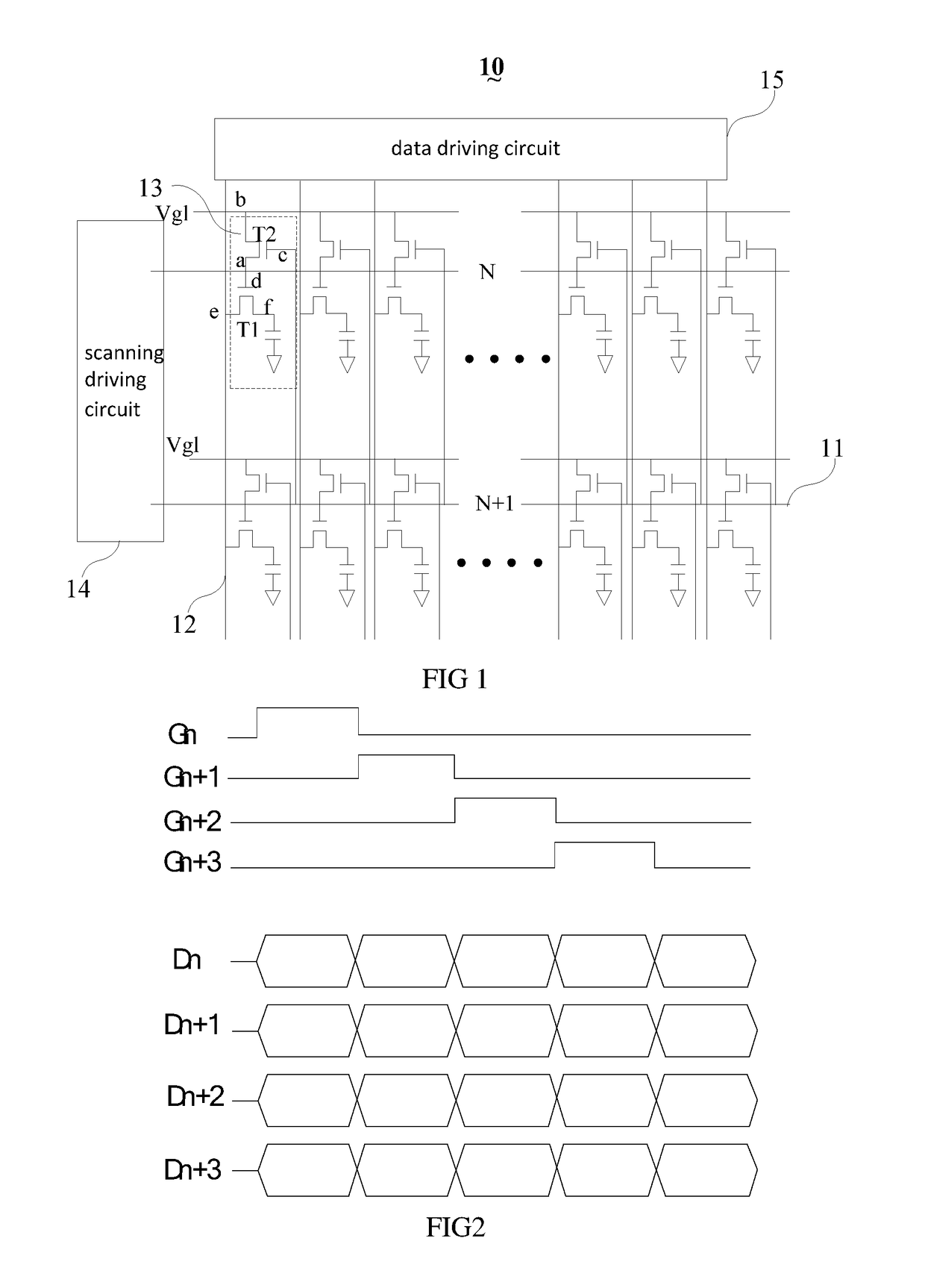
[0031]FIG. 1 is a schematic view of the array substrate in accordance with the present disclosure.

[0032]The array substrate 10 includes a plurality of scanning lines 11, a plurality of data lines 12, and at least one low voltage line (Vg1), wherein the scanning lines 11 and the data lines 12 intersect with other to form a plurality of pixel cells 13.

[0033]Each of the pixel cells 13 includes a first transistor (T1) for controlling a voltage of the pixel electrode within the array substrate 10. The at least one pixel cells 13 further includes a second transistor (T2) including a first end (a), a second end (b), and a control end (c), wherein the first end (a) connects to the control end (c) of the first transistor (T1), the control end (c) connects to the succeeding scanning line. The succeeding scanning line is turned on after the scanning line at a current level, which corresponds to the pixel cell 13 where the second transistor (T2) is located, is turned on. The second end (b) conn...

second embodiment

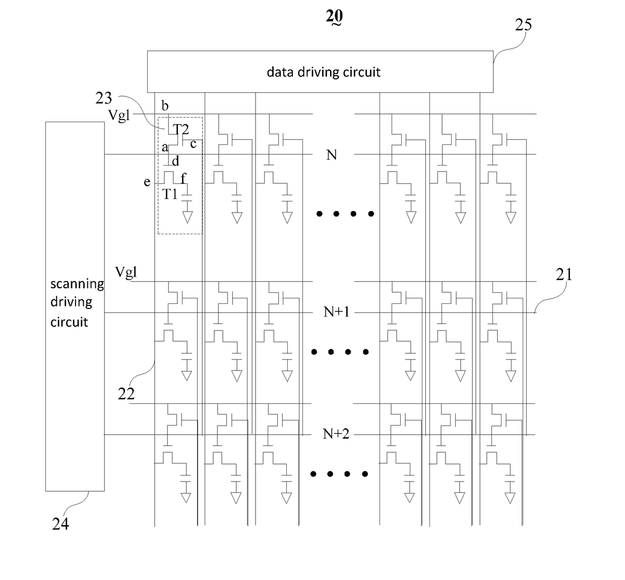
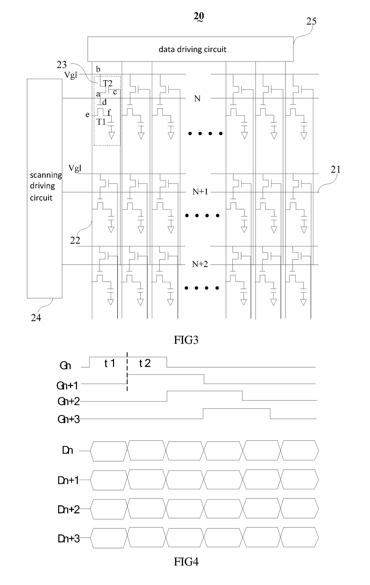
[0043]FIG. 4 is a schematic view showing timing sequence in accordance with the present disclosure. Also referring to FIG. 2, the pixel cell 23 at the N-th level is taken as one example. A falling edge of the scanning signals of the scanning line at the current level correspond to a rising edge of the scanning signals of the scanning line at the (N+2)-th level.

[0044]When a period of the rising edge of the scanning signals of the scanning lines 21 is too long, usually, a pre-charge driving method is adopted to charge the pixel circuit structure. With respect to the pre-charge driving method, before the scanning line at the current level is driven to find the address, the scanning driving circuit 24 provides the high potential to the scanning line at the current level to turn on the first transistor (T1) so as to conduct the pre-charge process to the pixel at the current level. As shown in FIG. 4, the half early period (t1) defined by the dashed line relates to the pre-charge period, ...

third embodiment

[0055]The control end of the second transistor (T2) of the pixel cell at the N-th level connects to the scanning line of the pixel cell at the (N+1)-th level. The succeeding scanning line in the third embodiment and the scanning line of the pixel cell at the N-th level are separated by the scanning line configured at least one level. The number of the scanning lines being arranged between the succeeding scanning line and the scanning line at the current level equals to a ratio of the pre-charging period to the normal charging period of the pixel cell where the second transistor (T2) is located. In the embodiment, the control end of the second transistor (T2) of the pixel cell at the N-th level connects to the scanning line of the pixel cell at the (N+2)-th level.

[0056]In FIG. 6, the array substrate 40 includes a plurality of scanning lines 41, a plurality of data lines 42, and at least one low voltage line (Vg1), wherein the scanning lines 41 and the data lines 42 intersect with oth...


PUM

PropertyMeasurementUnit
voltageaaaaaaaaaa
current levelaaaaaaaaaa
coloraaaaaaaaaa

Abstract

The present disclosure relates to an array substrate and a display panel. The array substrate includes a plurality of scanning lines, a plurality of data lines, and at least one low voltage line. The scanning lines and the data lines intersect with other to form a plurality of pixel cells. Each of the pixel cells includes a first transistor. At least one of the pixel cell further includes a second transistor having a first end, a second end, and a control end. The first end connects to the control end of the first transistor, and the control end connects to a succeeding scanning line. The succeeding scanning line is turned on after the scanning line at a current level is turned on, and the scanning line corresponds to the pixel cell where the second transistor is located.

Description

BACKGROUND OF THE INVENTION1. Field of the Invention[0001]The present disclosure relates to liquid crystal display (LCD) technology, and more particularly to an array substrate and a display panel.2. Discussion of the Related Art[0002]LCDs typically are characterized by attributes including thin, power-saving, and low radiation, and thus have been widely adopted by display products, such as TV, Monitor, Notebook, and App.[0003]With the increase of the resolution and the dimension of the LCDs, the charging rate of the LCDs is getting lower, which cannot satisfy the requirement of high resolution and large dimension.SUMMARY[0004]The present disclosure relates to an array substrate and a display panel for increasing the charging time period of the pixels so as to enhance the charging rate of the pixels and to reduce the risk of erroneous charging process. In this way, the display performance of the LCD may be enhanced.[0005]In one aspect, an array substrate includes: a plurality of sca...

Claims


Application Information

Patent Timeline
Patent Type & Authority Applications(United States)
IPC IPC(8): G02F1/1362G02F1/1368
CPCG02F1/13624G02F1/1368G02F1/136286
Inventor HAO, SIKUN
Owner TCL CHINA STAR OPTOELECTRONICS TECH CO LTD
Learn More