Light irradiation type heat treatment apparatus

Inactive Publication Date: 2018-10-18
DAINIPPON SCREEN MTG CO LTD
View PDF3 Cites 6 Cited by
  • Summary
  • Abstract
  • Description
  • Claims
  • Application Information

AI Technical Summary

Benefits of technology

[0012]Part of the light entering the light diffusion plate is diffused toward a peripheral portion of the substrate. This increases the in-plane uniformity of an illuminance distribution on the substrate without wastefully consuming

Problems solved by technology

This results in a junction depth much greater than a required depth, which might constitute a hindrance to good device formation.
As a result, the in-plane distribution of illuminance becomes nonuniform, which in turn causes variations in temperature distribution.
However, such contrivance necessitates the adjustment of a large number of parts and set values.
It has been significantly difficult to attain the in-plane uniformity of the illuminance distribution meeting a required level.
The

Method used


Image

  • Light irradiation type heat treatment apparatus
  • Light irradiation type heat treatment apparatus
  • Light irradiation type heat treatment apparatus

Examples


first preferred embodiment

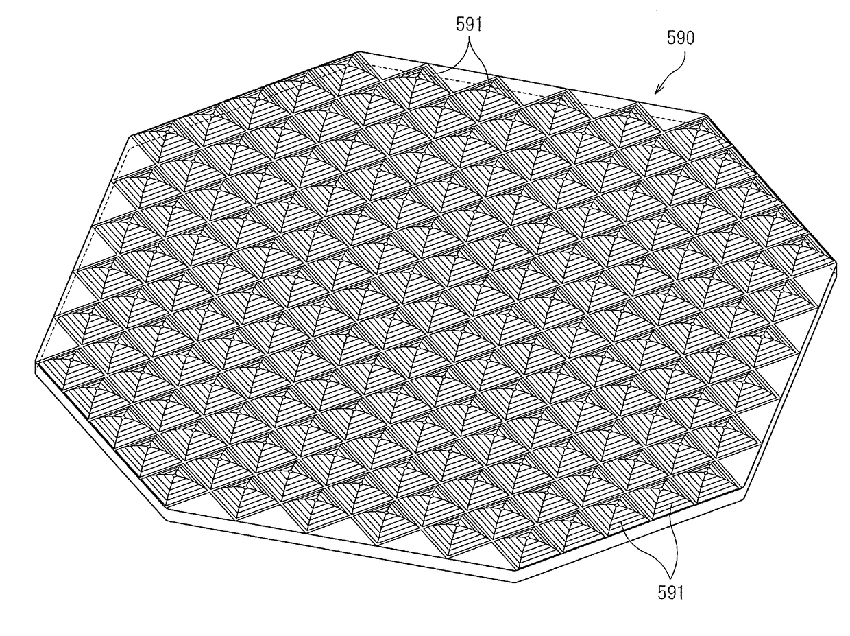
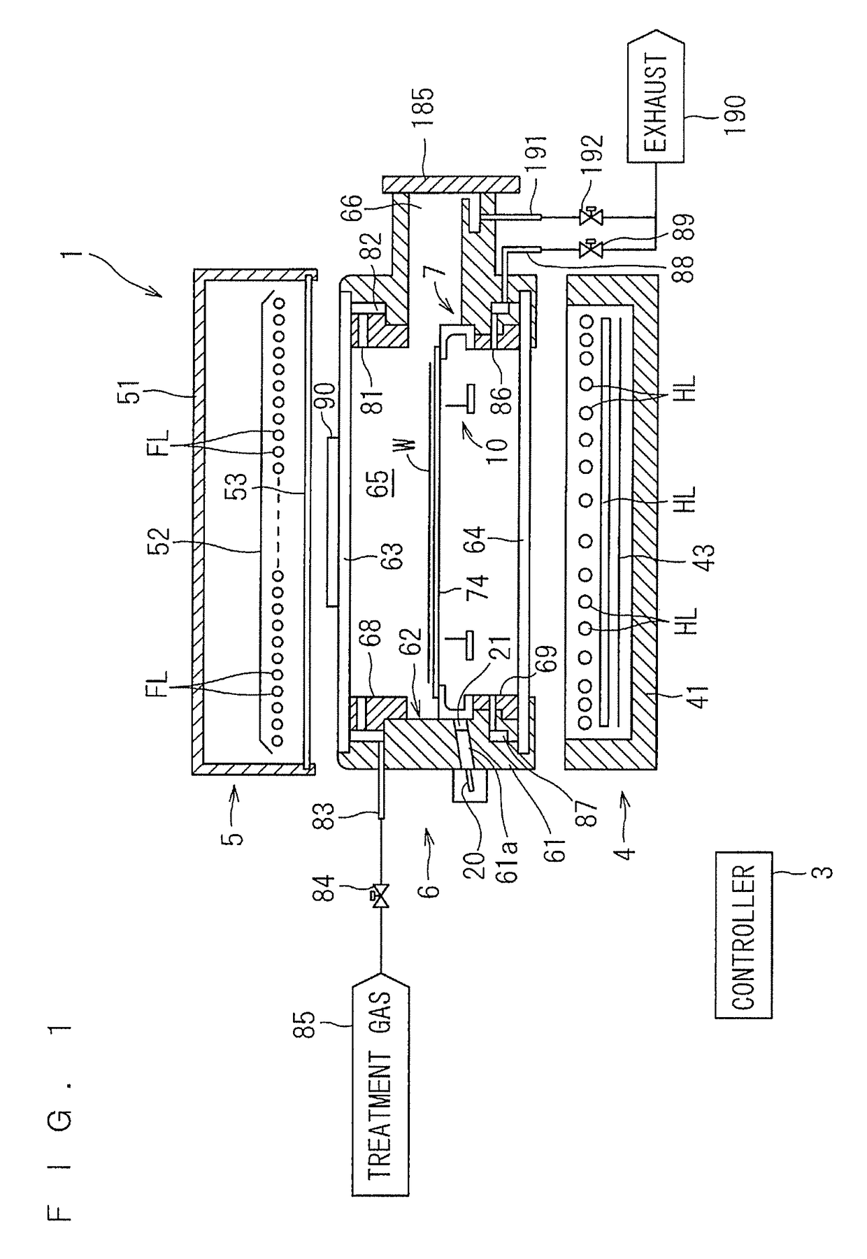
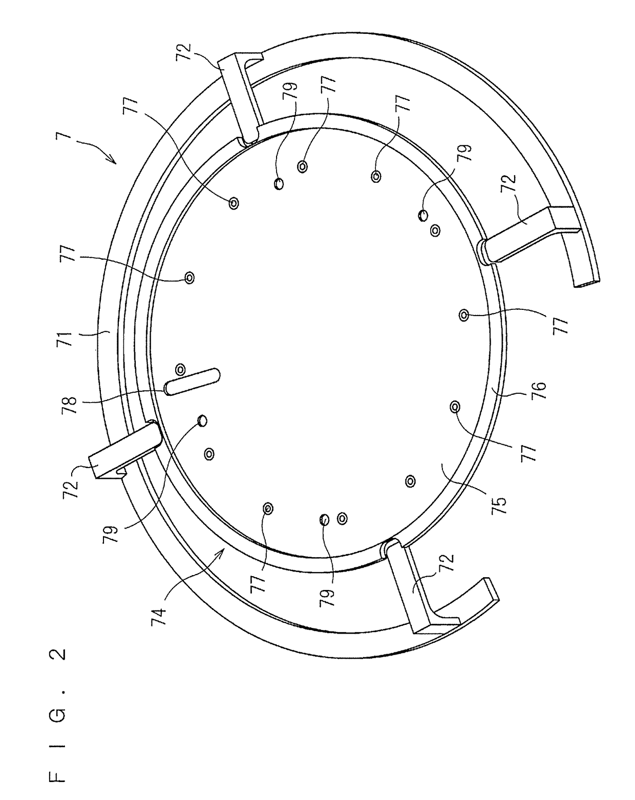
[0031]FIG. 1 is a longitudinal sectional view showing a configuration of a heat treatment apparatus 1 according to the present invention. The heat treatment apparatus 1 of FIG. 1 is a flash lamp annealer for irradiating a disk-shaped semiconductor wafer W serving as a substrate with flashes of light to heat the semiconductor wafer W. The size of the semiconductor wafer W to be treated is not particularly limited. For example, the semiconductor wafer W to be treated has a diameter of 300 mm and 450 mm (in the present preferred embodiment, 300 mm). The semiconductor wafer W prior to the transport into the heat treatment apparatus 1 is implanted with impurities. The heat treatment apparatus 1 performs a heating treatment on the semiconductor wafer W to thereby activate the impurities implanted in the semiconductor wafer W. It should be noted that the dimensions of components and the number of components are shown in exaggeration or in simplified form, as appropriate, in FIG. 1 and the ...

second preferred embodiment

[0083]Next, a second preferred embodiment according to the present invention will be described. The heat treatment apparatus 1 according to the second preferred embodiment is generally similar in overall configuration to that according to the first preferred embodiment. A procedure for the treatment of a semiconductor wafer W in the heat treatment apparatus 1 according to the second preferred embodiment is also similar to that according to the first preferred embodiment. The second preferred embodiment differs from the first preferred embodiment in the form of the light diffusion plate.

[0084]FIG. 11 is a perspective view showing the entire external appearance of a light diffusion plate 290 according to the second preferred embodiment of the present invention. The light diffusion plate 290 according to the second preferred embodiment includes a circular quartz plate having an upper surface provided with a plurality of concave surfaces 291. The disk-shaped light diffusion plate 290 ha...

third preferred embodiment

[0088]Next, a third preferred embodiment according to the present invention will be described. The heat treatment apparatus 1 according to the third preferred embodiment is generally similar in overall configuration to that according to the first preferred embodiment. A procedure for the treatment of a semiconductor wafer W in the heat treatment apparatus 1 according to the third preferred embodiment is also similar to that according to the first preferred embodiment. The third preferred embodiment differs from the first preferred embodiment in the form of the light diffusion plate.

[0089]FIG. 12 is a perspective view showing the entire external appearance of a light diffusion plate 390 according to the third preferred embodiment of the present invention. The light diffusion plate 390 according to the third preferred embodiment includes a circular quartz plate having an upper surface provided with a plurality of concave surfaces 391. The disk-shaped light diffusion plate 390 has a di...


PUM


Abstract

A light diffusion plate made of quartz and provided with a plurality of recessed spherical surfaces is placed on an upper chamber window so as to be in opposed relation to a central portion of a semiconductor wafer. Flashes of light emitted from flash lamps and passing by the side of the light diffusion plate impinge upon a peripheral portion of the semiconductor wafer. On the other hand, flashes of light emitted from the flash lamps and entering the light diffusion plate are diverged by the recessed spherical surfaces. Part of the light entering the light diffusion plate is diffused toward the peripheral portion of the semiconductor wafer. As a result, this increases the amount of light impinging upon the peripheral portion of the semiconductor wafer, and decreases the amount of light impinging upon the central portion of the semiconductor wafer. Thus, the in-plane uniformity of an illuminance distribution on the semiconductor wafer is increased.

Description

BACKGROUND OF THE INVENTIONField of the Invention[0001]The present invention relates to a heat treatment apparatus which irradiates a thin plate-like precision electronic substrate (hereinafter referred to simply as a “substrate”) such as a semiconductor wafer with light to heat the substrate.Description of the Background Art[0002]In the process of manufacturing a semiconductor device, impurity doping is an essential step for forming a pn junction in a semiconductor wafer. At present, it is common practice to perform impurity doping by an ion implantation process and a subsequent annealing process. The ion implantation process is a technique for causing ions of impurity elements such as boron (B), arsenic (As) and phosphorus (P) to collide against the semiconductor wafer with high acceleration voltage, thereby physically implanting the impurities into the semiconductor wafer. The implanted impurities are activated by the subsequent annealing process. When annealing time in this anne...

Claims


Application Information

Patent Timeline
IPC IPC(8): H01L21/67G02B5/02H05B3/00
CPCH01L21/67115G02B5/0215H05B3/0047H01L21/67248H01L21/6875G02B5/0231H01L21/67103H01L21/67109
Inventor NISHIDE, NOBUHIKO
Owner DAINIPPON SCREEN MTG CO LTD
Why Eureka
Try Eureka