Package structure and manufacturing method thereof

a technology of packaging structure and manufacturing method, which is applied in the direction of semiconductor devices, semiconductor/solid-state device details, electrical apparatus, etc., can solve the problems of increasing the risk of malfunction or failure of electronic chips due to cracks or warpages, so as to reduce the risk of failure, the effect of reducing the risk of failur

Inactive Publication Date: 2018-10-18
POWERTECH TECHNOLOGY
View PDF7 Cites 8 Cited by
  • Summary
  • Abstract
  • Description
  • Claims
  • Application Information

AI Technical Summary

Benefits of technology

[0004]Accordingly, the present invention is directed to a package structure and a manufacturing method thereof, which can lower the risk of malfunction or failure of a package structure of the chip and enhance the reliability thereof.
[0007]Base on the above, the protection layer is formed on the rear surface of the chip. Accordingly, the chip is strengthened to sufficiently alleviate the warpage issues during the manufacturing process of the package structure. Moreover, since the issues of the warpage of the chip are alleviated, the flip-chip bonding yield may be improved to avoid the non-joint issue. As result, the overall strength of the chip having the protection layer disposed thereon is enhanced.

Problems solved by technology

As the products gradually shrinkage in volume, the risk of malfunction or failure of the electronic chip due to crack or warpage is increased accordingly.
As such, how to miniature the package structure while maintaining the reliability and the functionality of the package, so as to lower the risk of failure of the final products, has become a challenge to those researchers in the field.

Method used


Image

  • Package structure and manufacturing method thereof
  • Package structure and manufacturing method thereof
  • Package structure and manufacturing method thereof

Examples


Embodiment Construction

[0014]Reference will now be made in detail to the present preferred embodiments of the invention, examples of which are illustrated in the accompanying drawings. Wherever possible, the same reference numbers are used in the drawings and the description to refer to the same or like parts.

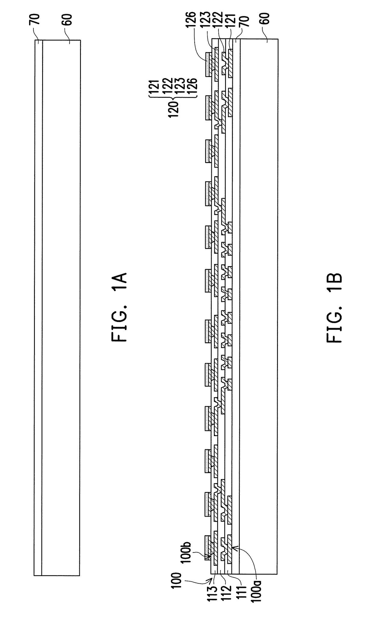
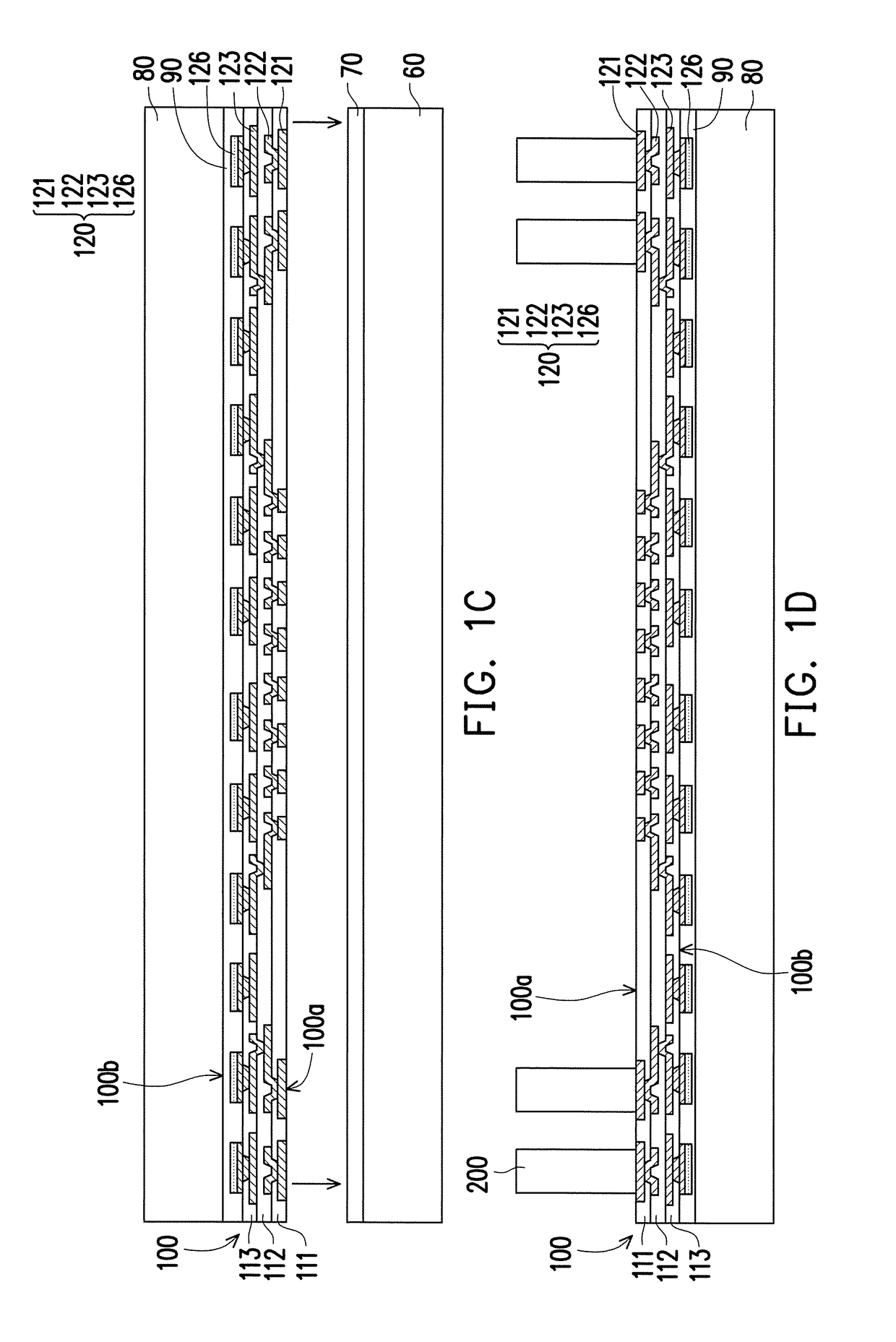
[0015]FIG. 1A to FIG. 1J are schematic cross-sectional view illustrating a manufacturing method of package structure according to an embodiment of the present invention. Referring to FIG. 1A, a first carrier substrate 60 is provided. In the embodiment, the first carrier substrate 60 may be made of silicon, polymer or other suitable materials. A first release layer 70 is formed on the first carrier substrate 60 to enhance the adhesion between the first carrier substrate 60 and the other structures subsequently formed thereon, and to improve the rigidity of the overall package structure during the manufacturing process. The first release layer 70 is, for example, a light to heat conversion (LTHC) adhes...


PUM


Abstract

A package structure includes a first redistribution structure, a chip, an insulation encapsulation and a protection layer. The first redistribution structure has a first surface and a second surface opposite to the first surface. The chip is disposed on the first surface of the first redistribution structure and has an active surface and a rear surface opposite to the active surface. The insulation encapsulation encapsulates the chip and the first surface of the first redistribution structure. The protection layer is directly disposed on the rear surface of the chip.

Description

CROSS REFERENCE TO RELATED APPLICATION[0001]This application claims the priority benefit of U.S. provisional application Ser. No. 62 / 484,907, filed on Apr. 13, 2017. The entirety of the above-mentioned patent application is hereby incorporated by reference herein and made a part of specification.BACKGROUND OF THE INVENTION1. Field of the Invention[0002]The present invention generally relates to a package structure and a display, in particular, to a package structure having a protection layer.2. Description of Related Art[0003]With advancement of the technology, the electronic product has been designed to achieve being light, slim, short, and small, so as to develop products that are smaller in volume, lighter in weight, higher in integration, and more competitive in the market. As the products gradually shrinkage in volume, the risk of malfunction or failure of the electronic chip due to crack or warpage is increased accordingly. As such, how to miniature the package structure while...

Claims


Application Information

Patent Timeline
Patent Type & Authority Applications(United States)
IPC IPC(8): H01L23/538H01L23/31H01L23/00H01L21/48H01L21/683H01L21/56
CPCH01L23/5389H01L23/5386H01L23/3128H01L23/3135H01L23/5383H01L24/16H01L23/5384H01L24/32H01L21/4857H01L21/6835H01L21/568H01L21/486H01L24/81H01L24/73H01L2221/68345H01L2221/68359H01L2224/16227H01L2224/32225H01L2224/73204H01L25/105H01L2225/1041H01L2225/1023H01L2225/107H01L2924/3025H01L2924/3511H01L2225/1058H01L21/4846H01L23/498H01L2224/81005H01L2221/68318H01L2221/68368H01L23/49822H01L23/49816H01L2224/81193H01L2224/131H01L2224/92125H01L2224/83104H01L24/83H01L24/13H01L2224/83005H01L2924/181H01L2224/9202H01L2924/014H01L2924/00014H01L2224/16225H01L2924/00H01L21/4853H01L21/563H01L2224/81191
Inventor CHANG CHIEN, SHANG-YUHSU, HUNG-HSINLIN, NAN-CHUN
Owner POWERTECH TECHNOLOGY
Why Eureka
Try Eureka